1.2 Introduction to the PDKs
Table of contents
Introduction to PDK
A Process Design Kit (PDK) is a crucial component in the semiconductor industry, used to model a fabrication process for the design tools that are used to create an integrated circuit. The PDK is created by the foundry, which defines a certain technology variation for their processes. It is then passed on to their customers to use in the design process.
Previously, PDK data is proprietary which is protected behind the non-disclosure agreement. Proprietary PDK data and commercial EDA tools are two main roadblocks in Integrated Circuit Design and Collaboration because it prevents the design to be shared among partners.
The use of open-source PDKs such as IHP SG13G2, GF180MCU and SKY130 has significantly reduced the cost of IC design, making it accessible to more people. The Google-sponsored Open Multi Project Wafer, or Open MPW, Shuttle Program has enabled market-relevant designs to be fabricated by people who traditionally would not have had the opportunity to design a chip.
Contents of a PDK
A typical PDK contains:
- A primitive device library: a collection of basic components that are used in the design process.
- Symbols: graphical representations of the components in the library.
- Device parameters: specific characteristics of the devices in the library.
- PCells or parameterized cells which are circuit elements that can be adjusted based on the needs of the design.
- Verification checks including Design Rule Checking (DRC), Layout Versus Schematic (LVS), Antenna and Electrical rule check.
- Technology data including layers, layer names, layer/purpose pairs, colors, fills, and display attributes.
- Process constraints: the limitations imposed by the fabrication process.
- Technology files for EDA tools.
- Simulation models of primitive devices (SPICE or SPICE derivatives): models used for simulating the behavior of the devices.
The PDK may also include standard cell libraries from the foundry, a library vendor, or developed internally. These libraries can include LEF format of abstracted layout data, symbols, library (.lib) files, and GDSII layout data.
The data in the PDK is specific to the foundry’s process. An accurate PDK will increase the chances of first-pass successful silicon. Therefore, a PDK is a critical tool in IC design, providing the necessary information and resources to design, simulate and verify the design before handing the design back to the foundry to tape out.
IHP SG13G2 PDK
IHP SG13 Options
| SiGe-HBT | SG13S | SG13G2 | SG13G3Cu | |
|---|---|---|---|---|
| fT / fmax | 250 / 340 GHz | 350 / 450 GHz | 470 / 650 GHz | |
| WEmitter | 170 nm | 130 nm | 110 nm | |
| HBT BVCEO | 1.7 V | 1.6 V | 1.5 V | |
| CMOS node | 130 nm | 130 nm | 130 nm | |
| Active devices | Schottky diodes, Antenna diodes, PN diodes, ESD | Schottky diodes, Antenna diodes, PN diodes, ESD | Schottky diodes, Antenna diodes, PN diodes, ESD | |
| Varactors | NMOS Varactor | NMOS Varactor | NMOS Varactor | |
| Resistors | Poly-Si, Thin Film | Poly-Si, Thin Film | Poly-Si | |
| MIM Caps | 1.5 fF / µm² (Al), 2.1 fF / µm² (Cu) | 1.5 fF / µm² (Al), 2.1 fF / µm² (Cu) | 2.1 fF / µm² | |
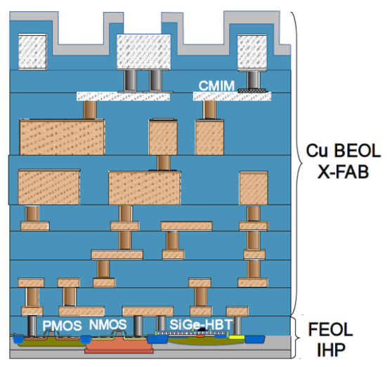
| Metallization | 7 Layers AL incl. 2 & 3 µm layers or *Cu: 4 + 2 (3µm), AL: 2 (3µm) | 7 Layers AL incl. 2 & 3 µm layers or *Cu: 4 + 2 (3µm), AL: 2 (3µm) | 7 Layers AL incl. 2 & 3 µm layers or *Cu: 4 + 2 (3µm), AL: 2 (3µm) | *Cu BEOL from X FAB |
PDK Contents
PDK tech files for opensource tools
-
DRC/LVS with KLayout
-
DRC/Extraction with Magic
-
Model files for Xyce / NgSpice
-
Symbols for Xschem / Qucs-S
-
Tech files for digital flow with OpenRoad
-
Electromagnetic estimation with OpenEMS
IO Cells
Primitive cells’ layout
Single-port SRAM
Standard cells
-
HV CMOS
-
LV CMOS
ihp-sg13g2
├── sg13g2_io
│   ├── cdl
│   ├── doc
│   ├── gds
│   ├── lef
│   ├── lib
│   ├── spice
│   ├── verilog
│   └── xschem
├── sg13g2_pr
│   └── gds
├── sg13g2_sram
│   ├── cdl
│   ├── doc
│   ├── gds
│   ├── lef
│   ├── lib
│   └── verilog
└── sg13g2_stdcell
    ├── cdl
    ├── doc
    ├── gds
    ├── lef
    ├── lib
    ├── spice
    └── verilog
IHP-Open-PDK/ihp-sg13g2/libs.tech
├── digital @ 9a6e7c9
├── klayout
├── magic
├── netgen
├── ngspice
├── openems
├── openroad
├── qucs
├── verilog-a
├── xschem
└── xyce/models
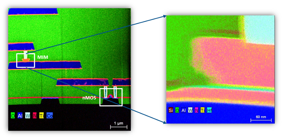
Transistor Structure & Metal Scheme
TEM cross section of 1T-1R Test strcture fabricated in 130m CMOS technology of IHP
- Metal scheme
References
- IHP SG13G2 PDK documentation
- IHP Open Design libraries
- Tim Ansell, Google/Skywater-pdk – Open source manufacturable PDK for Skywater 130nm process node, 2020. Video.
- Tim Edwards, Introduction to the SkyWater PDK, 2021.