3.1.3 An inverter schematic in Xschem with Skywater 130nm
Table of contents
Schematic capture
Prerequisites
- Finish the installation for analog design
Xschem basics
Keyboard shortcuts for xschem:
Shift + i: insert symbolq: Edit attributes (when a symbol is selected)Alt + r: rotate symbolsAlt + f: mirror symbolw: create wire to connect two pointsm: move a selected objectsc: copy the selected object
Create inverter schematic
1. Ensure that the environment variable PDK_ROOT and PDK point to the correct directory and pdk folder.
echo $PDK_ROOT
echo $PDK
If it has not been set yet, you can set it by using the following command in bash shell:
export PDK_ROOT=$PWD/unic-cass/pdks
export PDK=sky130A
2. Create a directory and copy the configuration file
Create a new directory named inverter and copy xschemrc into this directory
cd $HOME
mkdir -p unic-cass/inverter
cd unic-cass/inverter
cp -a $PDK_ROOT/$PDK/libs.tech/xschem/xschemrc .
echo 'set editor {gedit}' >> xschemrc # use gedit to edit the netlist
3. Run xschem
Run xschem from the command line inside the inverter directory
xschem
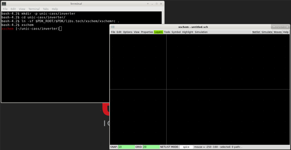
4. Insert a symbol into the schematic
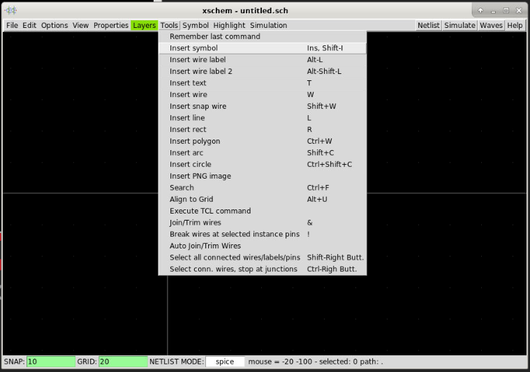
Insert nfet3_01v08 and pfet3_01v08 symbol in Xschem by selecting Tools >> Insert Symbol in the menu (or the keyboard shortcut Ins or Shift + I) .
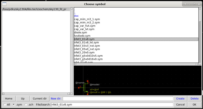
5. Add NFET symbol to the schematic
Browse to $PDK_ROOT/$PDK/libs.tech/xschem/sky130_fd_pr and select nfet3_01v8 and click OK to add the symbol of nfet3 into the schematic window.
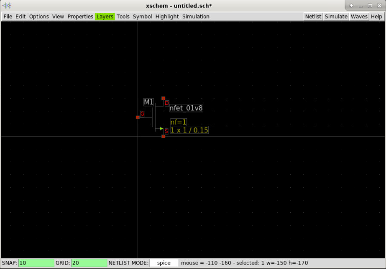
6. Place NFET’s symbol to the schematic
Click any place on the schematic window to place the nfet3 symbol as below:
7. Add PFET into the schematic
Repeat step 5 and step 6 with pfet3_01v8 to place the pfet into the schematic window.
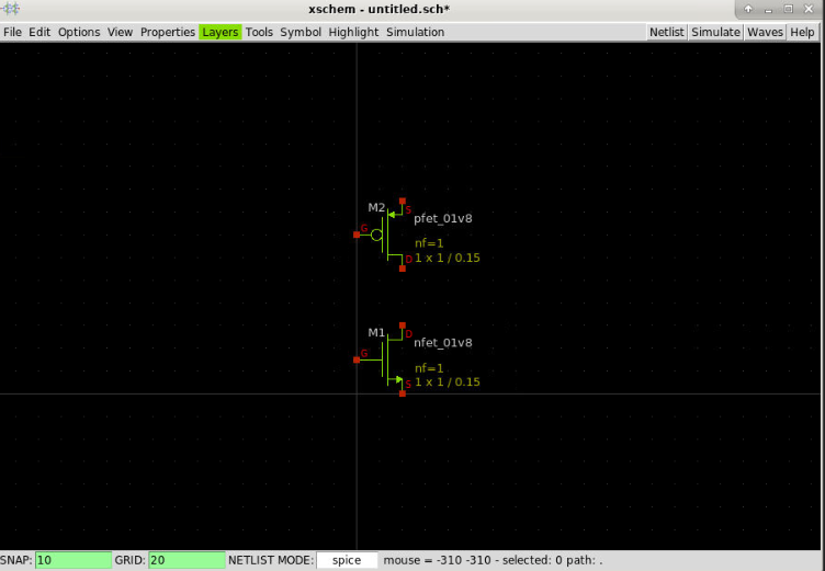
8. Wire two transistors to form an inverter
Next, we need to connect the two transistors to form an inverter. This can be done by move your cursor to the pin of one of the transistors pin, then press w shortcut and click on the pin that you want to connect as follow:
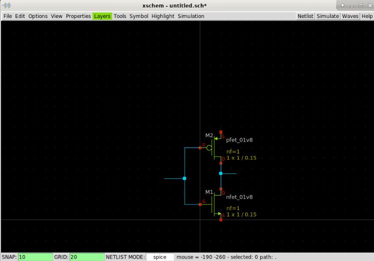
You should get acquainted with the w shortcut to do the wiring.
9. Connect power VDD and ground GND
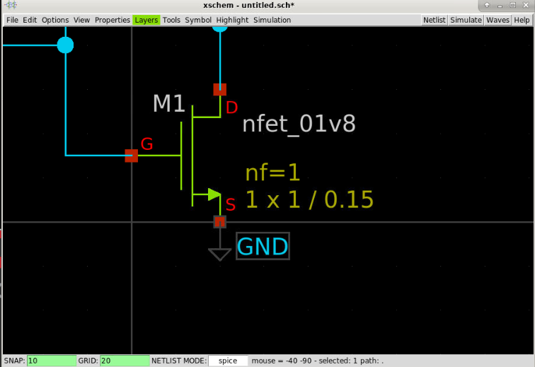
Next, we need some basic components such as VDD, GND and voltage sources to add to the schematic for simulation. This can be done by repeat the step 4 but selecting the default xschem_library/devices and add these devices into your schematic as bellow:
10. Add a voltage source
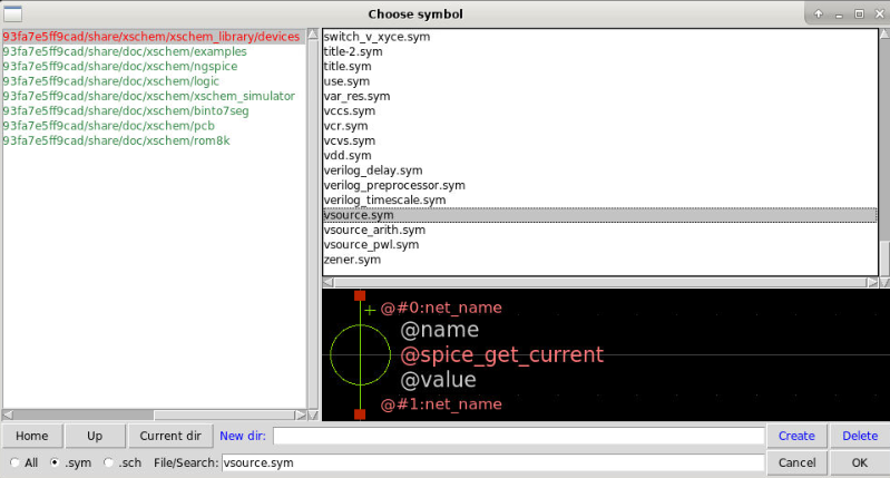
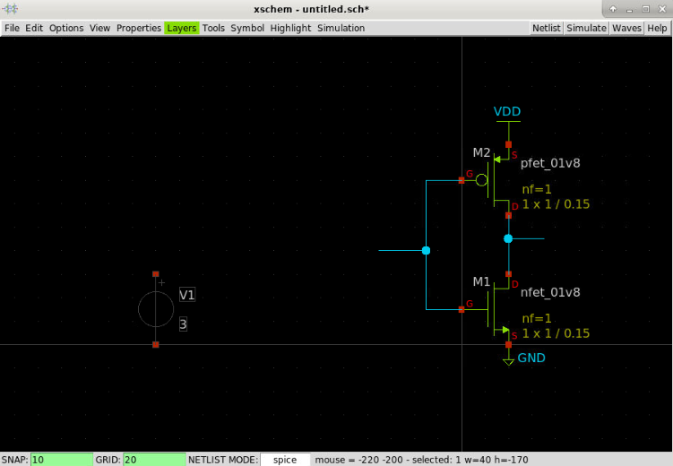
Next, we need to add a voltage source symbol (vsource.sym) into the schematic
11. Edit the voltage source’s properties
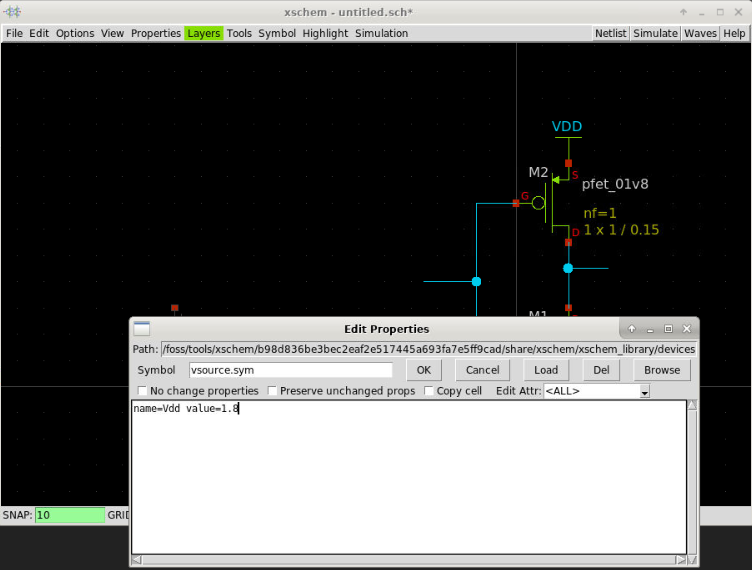
Next, we will have to edit the voltage source properties by right clicking on the voltage source and selecting “edit attributes” (or selecting the voltage source symbol and press q). Change the name to Vdd and the value to 1.8 (1.8V is the normalized voltage of skywater 130nm). Then, press OK.
12. Connect the voltage source to GND and VDD
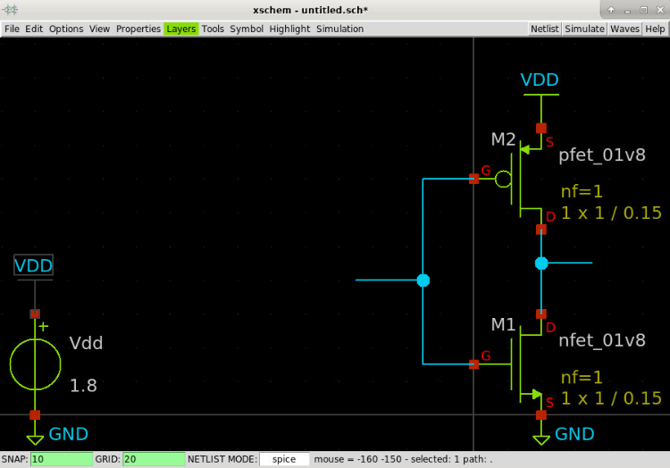
Next, we need to connect GND and VDD to the voltage source. The fastest way to do this is to copy the gnd symbol and vdd symbol by selecting the symbol, pressing c (shortcut for copying) and connecting it to the vsource symbol.
Create the testbench
Next, we build the testbench for the inverter circuit in xschem. We will learn how to create the lab pin to connect and monitor the signals during the simulation, using the vsource to create the supply voltage and the dc analysis.
Create the supply voltage
13. Create the input signal
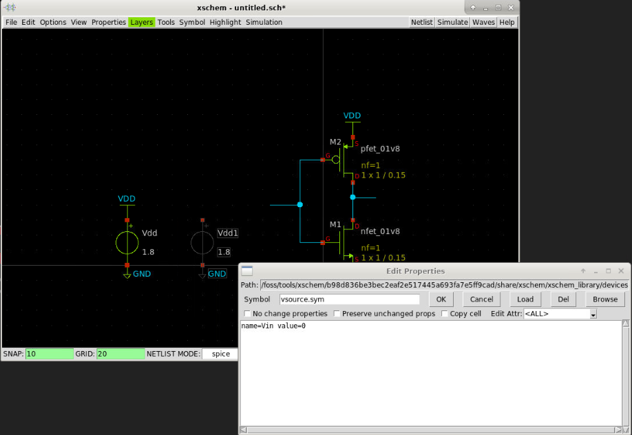
Next, we need to create another voltage source for the input signal. This can be done by copying the previous voltage source and editing its attributes. Use your mouse and select the vsource and GND symbols, press ‘c’ to copy and click to paste it.
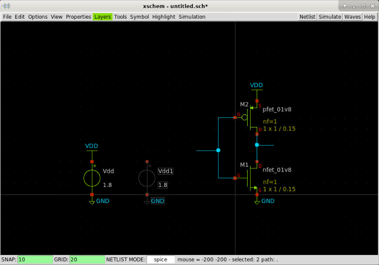
Select the vsource symbol that you’ve just created, press q to change its attributes as follows:
Name: Vin
Value: 0
Click OK.
Insert the model library and the simulation corner
14. Insert a code symbol to include the transistor model
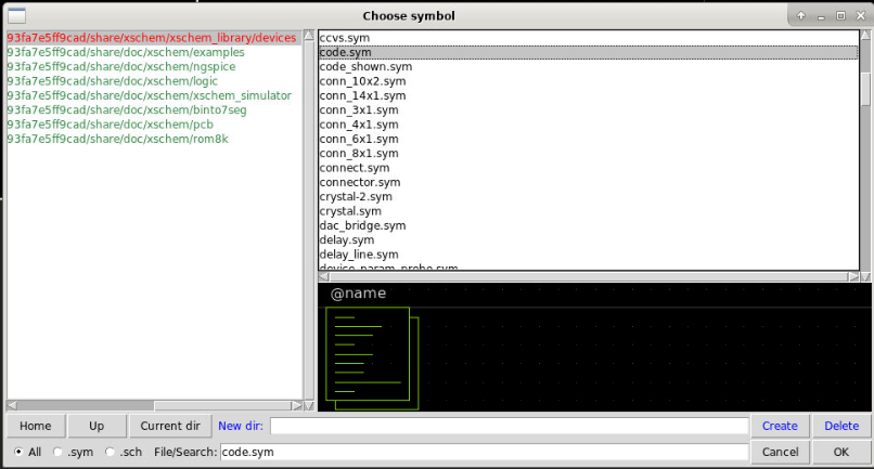
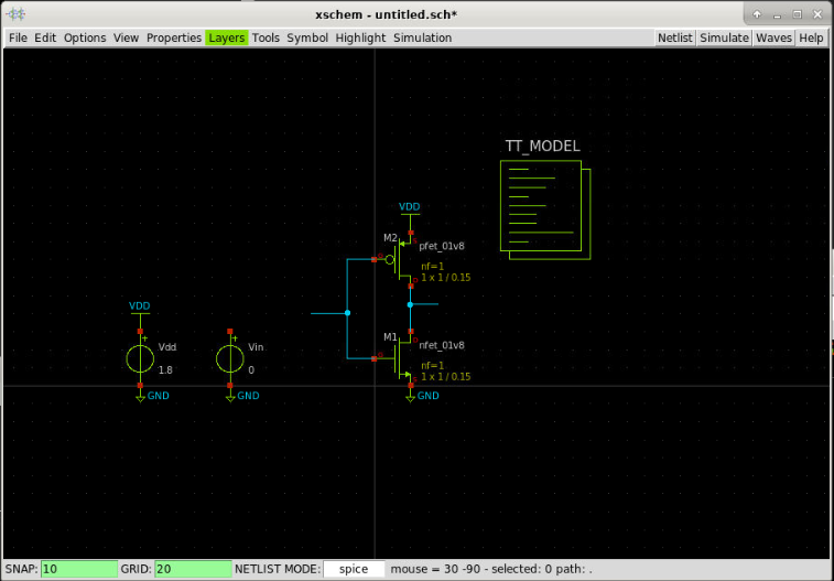
Next, we need to insert the simulation model into the schematic so that we can simulate the design using Ngspice. Press ‘Shift + i’ to insert the code symbol in the xschem device library then press OK to place it into xschem.
15. Enter the model details into the code symbol
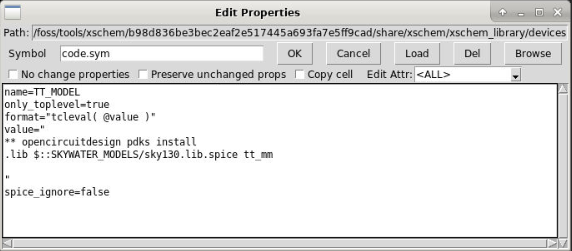
Select the newly created symbol, and change its properties as follows and press ‘OK’.
Setup DC analysis
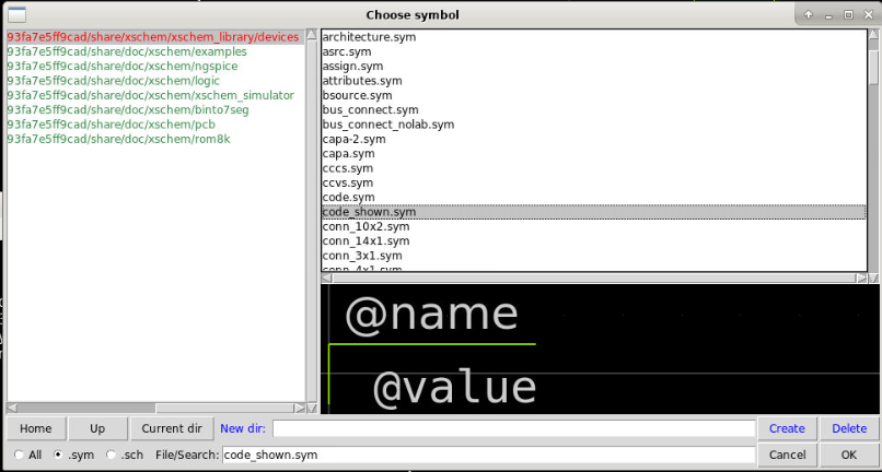
16. Insert a code_shown symoble to include the DC analysis
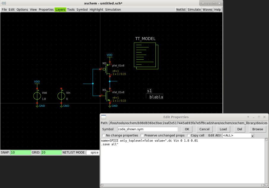
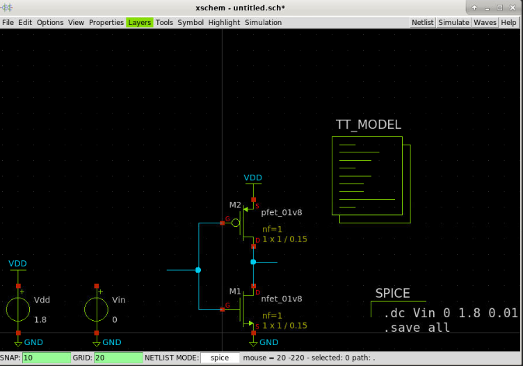
Next, we need to add a code_shown symbol and change it properties as follows:
Name: SPICE
Value: ".dc Vin 0 1.8 0.01
           .save all"
Then press OK.
Using lab pin to label net and monitor the simulation results
17. Insert a lab_pin
Next, we have to insert the lab_pin symbol for the input, the output and connect the input to the voltage source Vin. This can be done by pressing shift + i and selecting lab_pin.sym in the xschem device library.
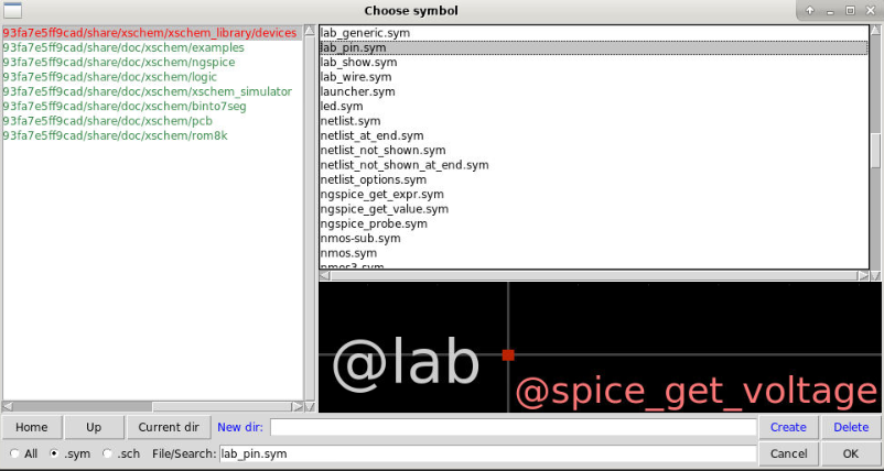
After that, we can attack it to the input by placing it on the input net.
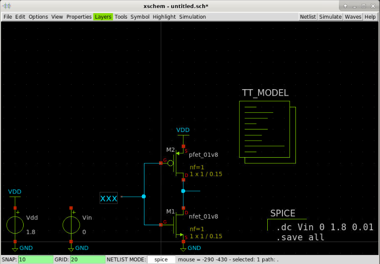
18. Name a lab_pin
Change the pin name to Vin by pressing on the lab_pin symbol, and press q. Change the name to Vin and press OK.
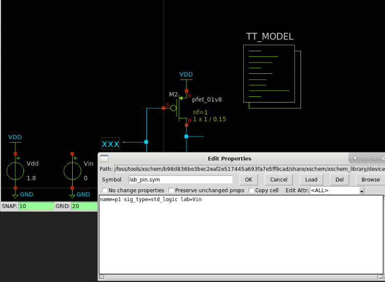
19. Create a new lab_pin by copying the old one
Copy Vin lab_pin symbol and connect it to the other end of the vsource symbol by selecting Vin lab_pin symbol, press c to copy and place it to the correct location. You can rotate the symbol by pressing alt + r
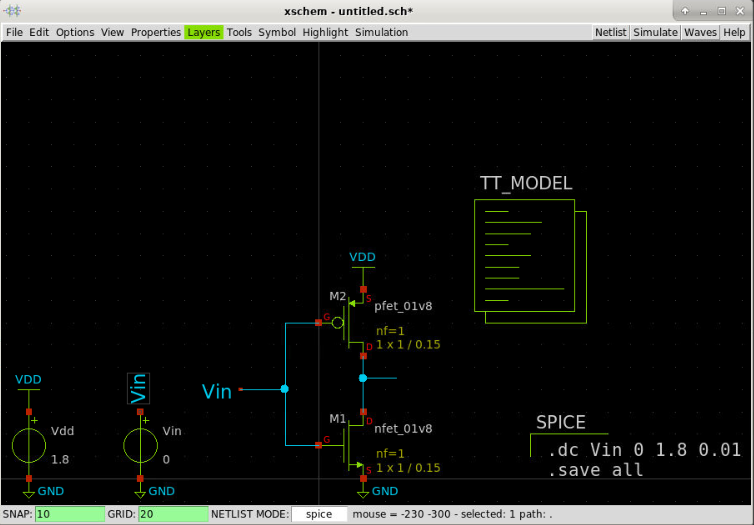
20. Create a lab_pin for Vout
The last step is to copy the Vin lab_pin symbol (select Vin lab_pin and press alt + f to mirror it) and place it on the output net. After that, we named it Vout.
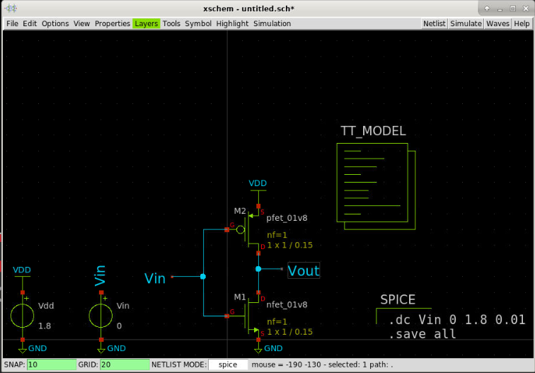
21. Save the schematic
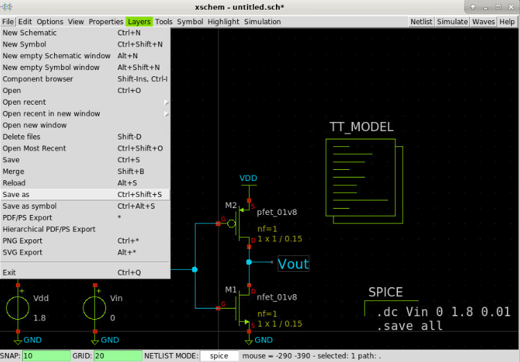
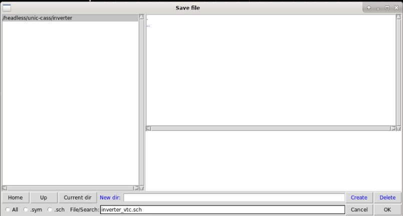
Now we can save the schematic into inverter.sch by click on File >> save as >> interver.sch
Create design netlist
22. Generate the netlist
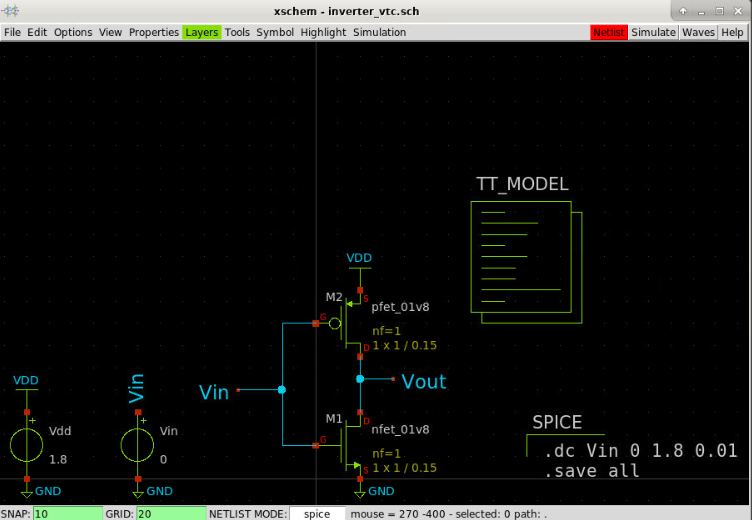
The schematic is done, next you can generate the netlist by click on netlist button
23. View/Edit the netlist
After the netlist is successfully generated (without warning or error in the info window), we can view our netlist by select Simulation >> Edit Netlist
** sch_path: /home/cass/unic-cass/inverter/xschem/inverter_vtc.sch
**.subckt inverter_vtc
XM1 Vout Vin GND GND sky130_fd_pr__nfet_01v8 L=0.15 W=1 nf=1 ad='int((nf+1)/2) * W/nf * 0.29' as='int((nf+2)/2) * W/nf * 0.29' pd='2*int((nf+1)/2) * (W/nf + 0.29)'
+ ps='2*int((nf+2)/2) * (W/nf + 0.29)' nrd='0.29 / W' nrs='0.29 / W' sa=0 sb=0 sd=0 mult=1 m=1
XM2 Vout Vin VDD VDD sky130_fd_pr__pfet_01v8 L=0.15 W=1 nf=1 ad='int((nf+1)/2) * W/nf * 0.29' as='int((nf+2)/2) * W/nf * 0.29' pd='2*int((nf+1)/2) * (W/nf + 0.29)'
+ ps='2*int((nf+2)/2) * (W/nf + 0.29)' nrd='0.29 / W' nrs='0.29 / W' sa=0 sb=0 sd=0 mult=1 m=1
Vdd VDD GND 1.8
Vin Vin GND 0
**** begin user architecture code

** opencircuitdesign pdks install
.lib /home/cass/unic-cass/pdks/sky130A/libs.tech/ngspice/sky130.lib.spice tt_mm


.dc Vin 0 1.8 0.01
.save all

**** end user architecture code
**.ends
.GLOBAL VDD
.GLOBAL GND
.end
Configure & run the simulation
24. Configure the simulator & tools
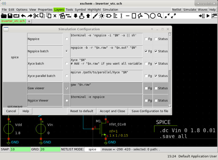
The simulation setup can be done by selecting Simulation >> Configure simulators and tools.
- In the Ngspice section, select
Ngspice batchto use ngspice batch mode. - In the
Spicewavesection, selectGaw Viewer - Click on
Accept and Close. You can also save the simulation option by clicking onSave Configurationto file
25. Simulate the design
To simulate the design, click on the Simulate button. If the simulate button is red, the simulator is running.
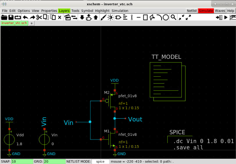
When the simulation finishes, a new window will appear with the simulation status. You should check it to see if there is any problem during the simulation.
Ngspice output
Completed: ngspice -b -r /home/cass/.xschem/simulations/inverter_vtc.raw /home/cass/.xschem/simulations/inverter_vtc.spice
data:

Note: No compatibility mode selected!


Circuit: ** sch_path: /home/cass/unic-cass/inverter/xschem/inverter_vtc.sch

binary raw file "/home/cass/.xschem/simulations/inverter_vtc.raw"
Doing analysis at TEMP = 27.000000 and TNOM = 27.000000

No. of Data Columns : 12

No. of Data Rows : 181

Total analysis time (seconds) = 0.002

Total elapsed time (seconds) = 5.131

Total DRAM available = 15402.340 MB.
DRAM currently available = 14062.492 MB.
Maximum ngspice program size =  153.242 MB.
Current ngspice program size =  137.582 MB.

Shared ngspice pages =    8.941 MB.
Text (code) pages =    5.496 MB.
Stack = 0 bytes.
Library pages =  137.090 MB.
Use Gaw to view the simulation waves
26. View simulation results
You can view the simulation results by clicking on the Waves button. A Gaw will be displayed with the recorded signals.
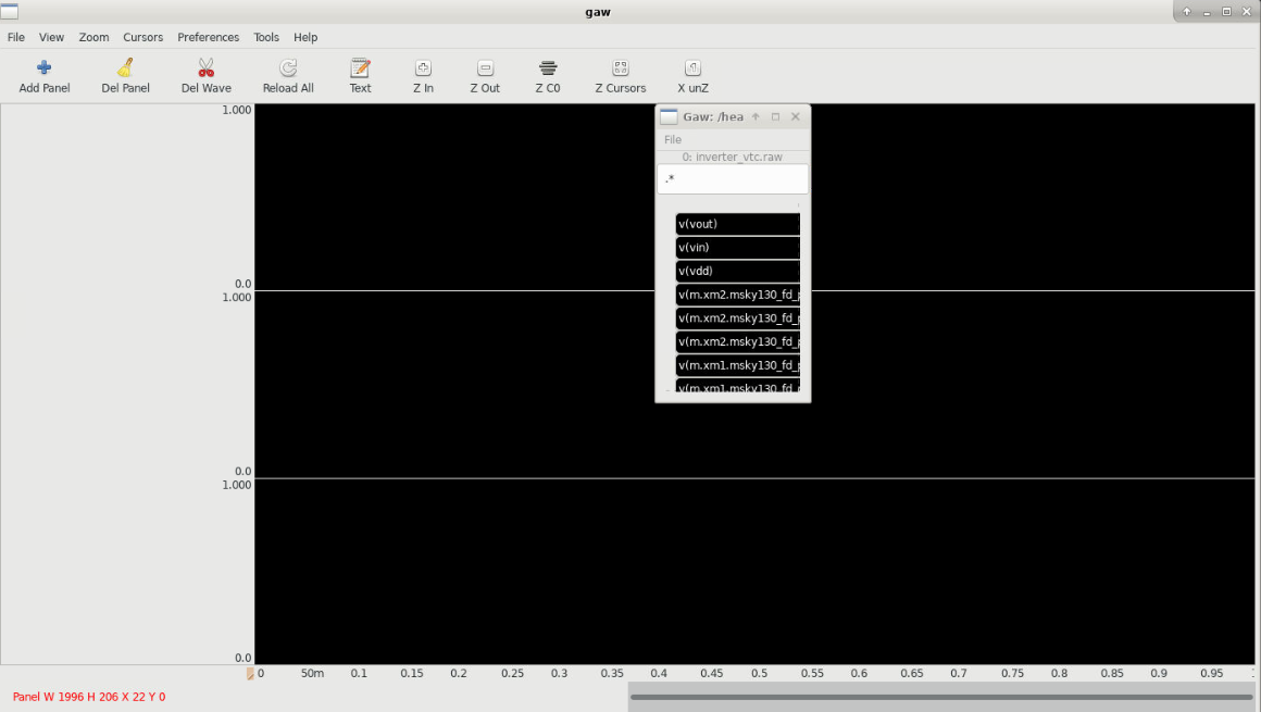
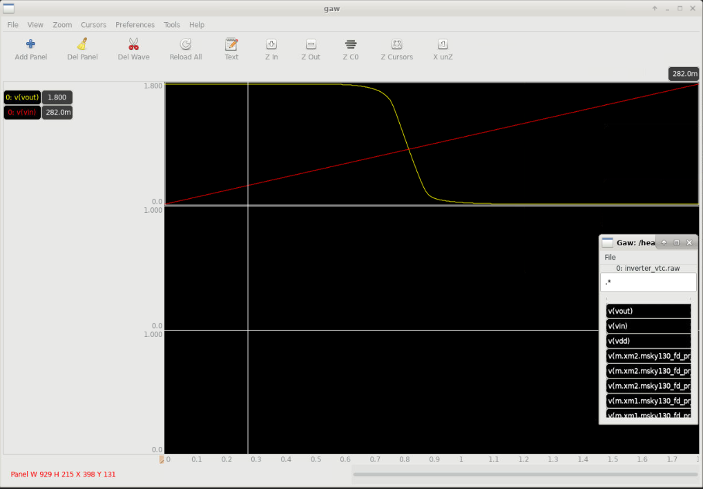
To add a signal to the wave viewer, you can click on a panel first, then add the signal in the signal list. For example, I add te Vin and Vout signals to the waveform as follows:
What’s next?
You’ve just finished the basic tutorials on how to draw schematics in Xschem and run the simulation in NGSpice. In real life, schematics are organized in hierarchy so that they can be easily reused and modified. In the next lesson, you will learn how to create a hierarchical schematic and how to draw a symbol in xschem.