3.1.5 Hierarchical schematic captures in Xschem & time domain simulation
Table of contents
Prerequisites
- Finish the installation for analog designs described in either Lesson 2.2 or Lesson 2.3
- Finish the previous lessons on the simulation of an inverter and creating its symbol.
PDK setup:
Ensure that the environment variable PDK_ROOT and PDK point to the correct directory and pdk folder.
echo $PDK_ROOT
echo $PDK
If it has not been set yet, you can set it by using the following command in bash shell:
export PDK_ROOT=$PWD/unic-cass/pdks
export PDK=sky130A
Create a new directory named ‘inverter’ and copy xschemrc into this directory
mkdir -p unic-cass/inverter
cd unic-cass/inverter
cp -a $PDK_ROOT/$PDK/libs.tech/xschem/xschemrc .
echo ‘set editor {gedit}’ >> xschemrc # use gedit to edit the netlist
Create a buffer schematic using two inverters
1. Create a new schematic for buffer design in Xschem
Create a new schematic in Xschem by selecting File >> new schematic.
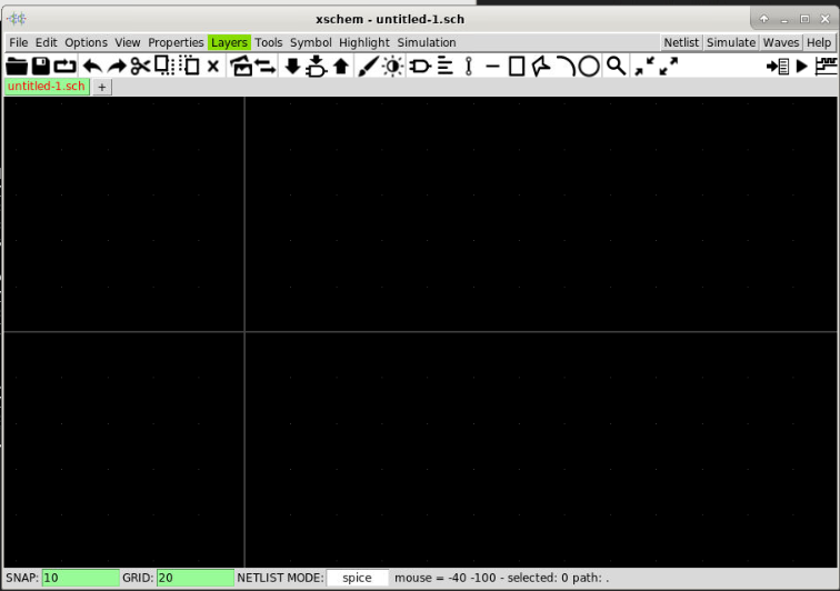
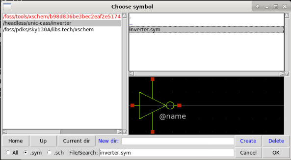
2. Insert the inverter symbol
Insert two inverter symbols by press the keyboard shortcut Shift + i or Ins as follows:
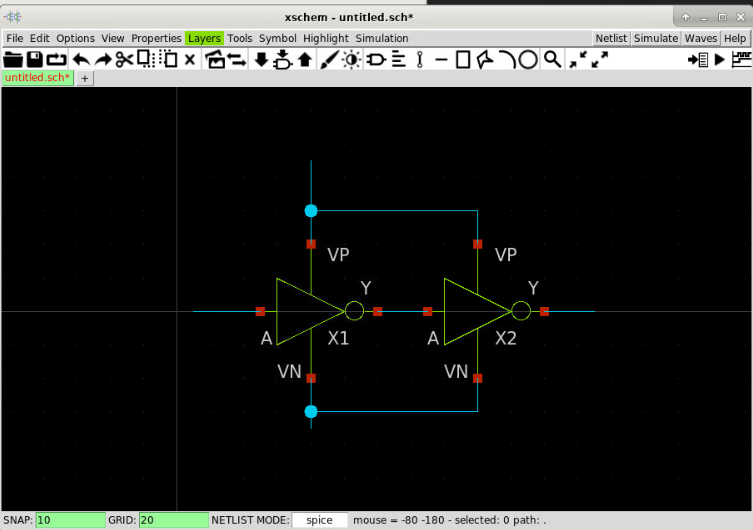
3. Wire two inverter to create a buffer
Now we need to create wires to connect these ports to form a buffer. This can be done by pointing your cursor to the point that you want to create the wire and pressing w to make a wire. Move your cursor to the point that you want to end the wire. Then, you can press w to make a new wire, and click on the stop. You can repeat this process multiple times until you have a circuit like the following.
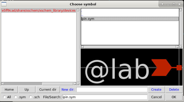
4. Create input, output and inout pins
Next, we create the input pin, output pin and the power supply pins as in the previous lesson. Just to recall, this can be done by inserting the ipin symbol for input pins, or opin symbol for the output pins and iopin symbol for the supply net. Don’t forget to change the name by selecting the pin and press ‘q’ shortcut to modify the name.
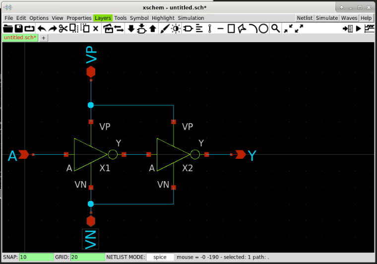
5. Save the buffer schematic
Next, we can save the schematic by selecting File >> Save as. Put the filename as buffer.sch and save it to the inverter directory and press OK.
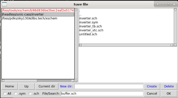
6. Create the buffer symbol
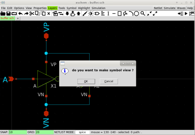
Now, we can create a symbol for the buffer. We take a different approach this time. Create a new symbol by selecting Symbol >> Make symbol from schematic. Xschem will ask us to change to the symbol view. Press OK on the pop-up menu.
7. Open the automatically generated symbol
Xschem will create a new file buffer.sym in the same directory with the buffer.sch. Now, we can open the symbol and modify it by selecting File >> Open. Then, we select buffer.sym.

8. Delete the default box to create a new shape
In the symbol windows, we will delete the box by selecting the lines and delete them.
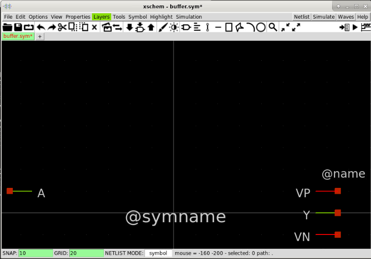
9. Organize the pins
Next, we organize the pin, the remaining line, and the pin text selecting them and move them to the correct position as the followings:
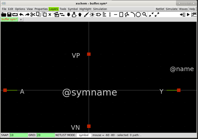
10. Draw a triangle for buffer symbol
Next, we draw the triangle as in the previous lesson.
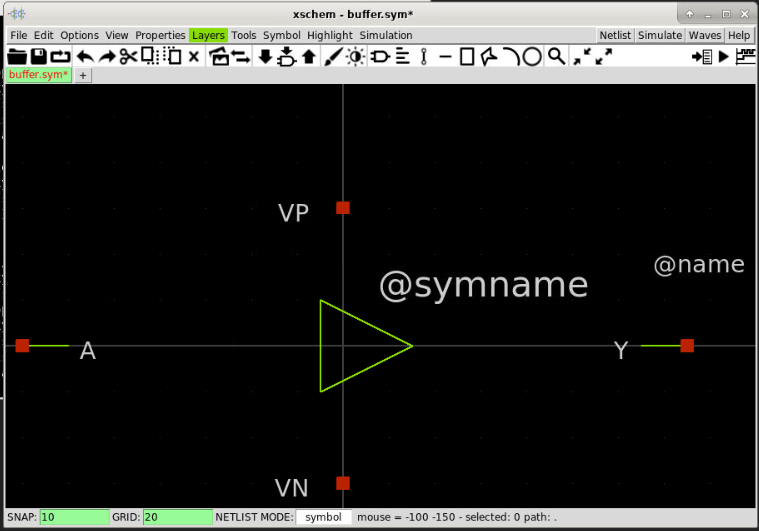
11. Move the pins and texts
Now you can move the pin, and the text by selecting them and press m and move the cursor to the desired position.
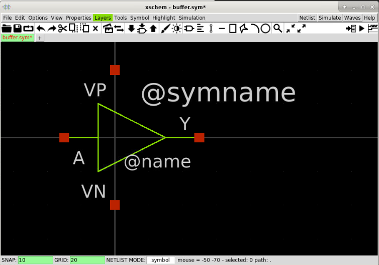
12. Draw lines
Next, we can draw the lines to connect the VN pin and VP pin to the triangle.
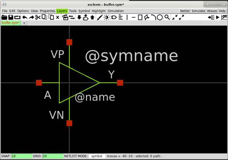
13. Save the symbol
Now, we can save the symbol by selecting File >> Save.
Create the buffer testbench
14. Create a new schematic to test the buffer design
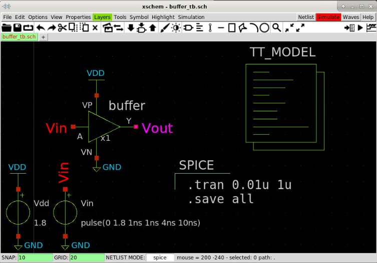
To verify the buffer behavior, we also need to create a testbench for it. In this lesson, we will do a time-domain simulation with the input as a square wave and verify the output. This can be done by creating a new schematic. Select File >> New schematic to open a new schematic window.
15. Insert the buffer design into the testbench
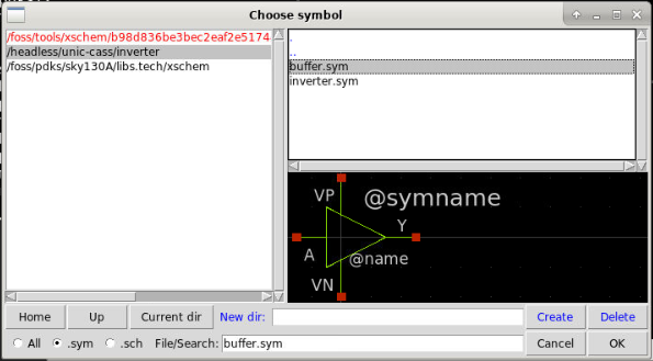
In search the buffer symbol by selecting Tools >> Insert symbol. Select the buffer symbol.
16. Create the power and ground nets
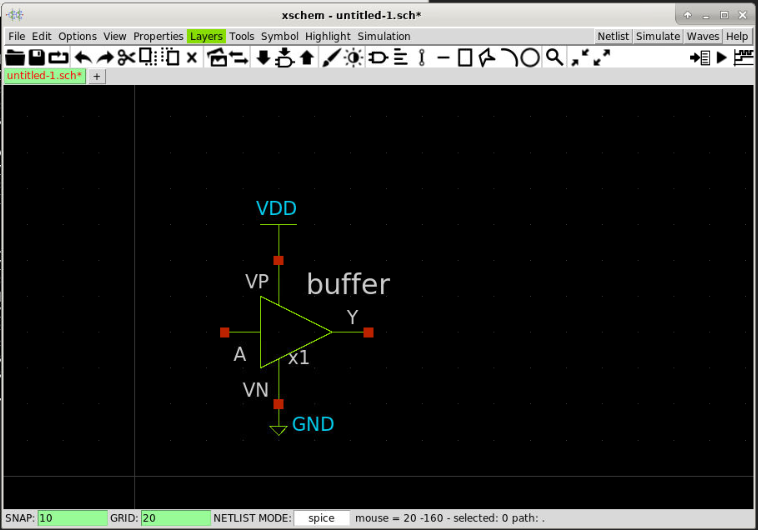
Next, we insert and connect the VDD symbol and GND symbol. Select Tools >> Insert symbol and select the vdd.sym and gnd.sym. Place them on the pin of the buffer. The results is as follow:
17. Create the voltage sources
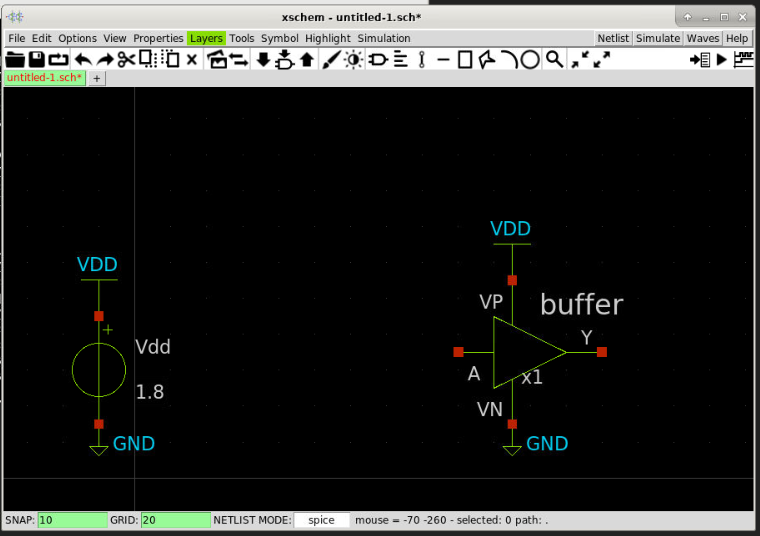
Next, we insert the vsource.sym and connect VDD and GND to its terminal to create 1.8V supply voltage. Please remember to edit the vsource.sym attribute to name=Vdd, and value=1.8.
18. Create the input signal
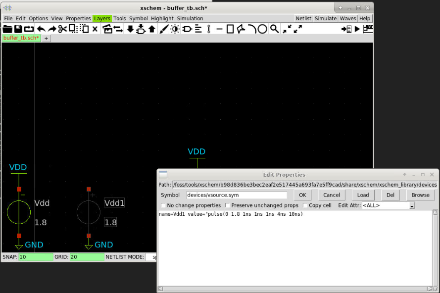
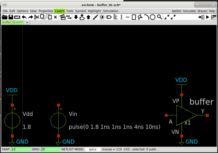
Now, we can copy the voltage source and GND by selecting them and use the keyboard shortcut c. Place it in a new place and change it properties as follows:
19. Create the lab pins for the input and the output
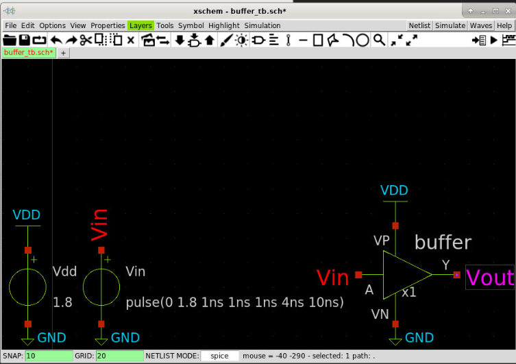
Next, we create two lab_pins one for the input and one for the output by inserting lab_pin.sym and rename it to Vin and Vout.
20. Include the model for simulation
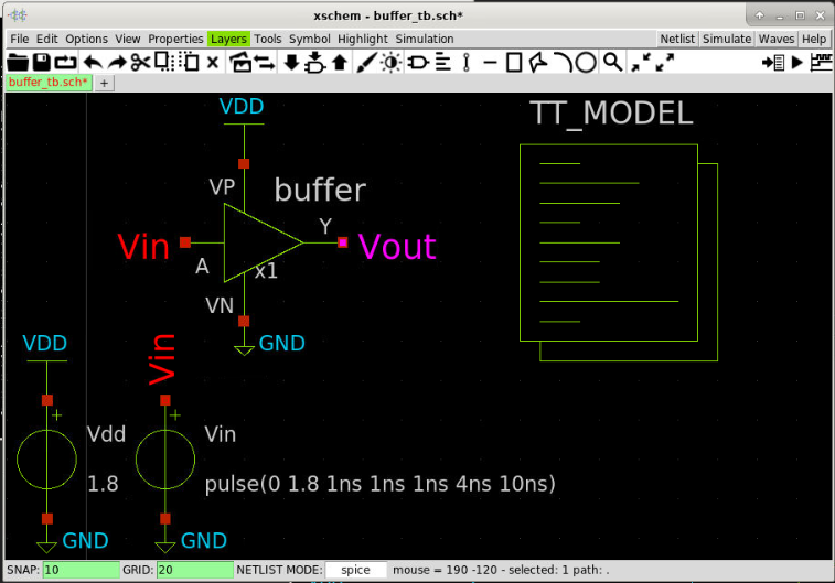
Next, we insert the TT_MODEL as in the previous lesson.
21. Insert the code symbol
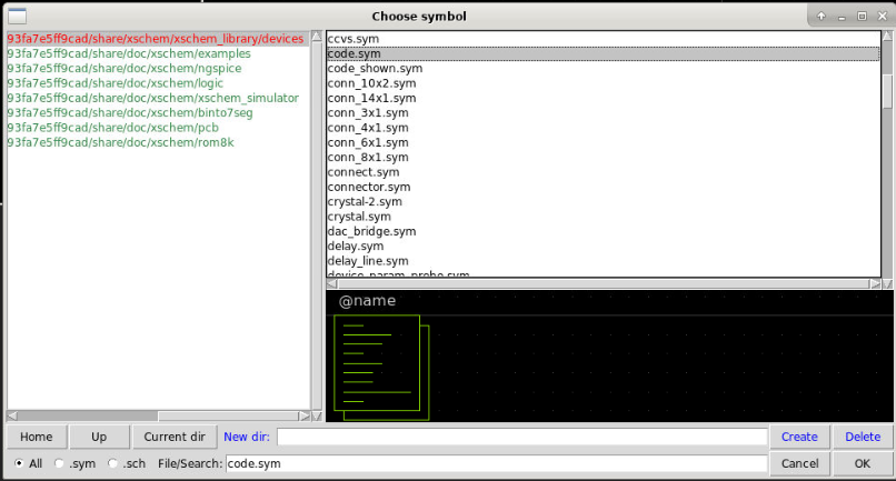
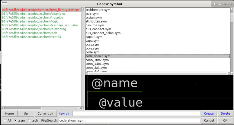
Press Shift + i to insert the code symbol in the xschem device library then press OK to place it into xschem.
22. Change its properties to include the simulation model
Select the newly created symbol, and change its properties as follows and press OK.
23. Set up analysis using code_shown symbol
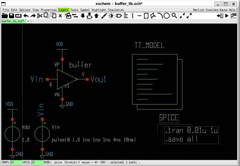
Next, we need to add a code_shown symbol and change it properties as follows:
Name: SPICE
Value: ".tran 0.01u 1u
           .save all"
Then press OK.
24. Save the schematic
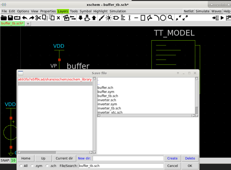
Now we can save the schematic into inverter.sch by click on File >> save as >> buffer_tb.sch
Create design netlist
25. Generate the testbench netlist
The schematic is done, next you can generate the netlist by click on netlist button After the netlist is successfully generated (without warning or error in the info window), we can view our netlist by select Simulation >> Edit Netlist.
Output netlist:
Output netlist
** sch_path: /home/cass/unic-cass/inverter/buffer_tb.sch
**.subckt buffer_tb
x1 VDD Vin Vout GND buffer
Vdd VDD GND 1.8
Vin Vin GND pulse(0 1.8 1ns 1ns 1ns 4ns 10ns)
**** begin user architecture code

** opencircuitdesign pdks install
.lib /home/cass/eda/unic-cass/share/pdk/sky130A/libs.tech/ngspice/sky130.lib.spice tt_mm


.tran 0.01u 1u
.save all

**** end user architecture code
**.ends

* expanding   symbol:  buffer.sym # of pins=4
** sym_path: /home/cass/unic-cass/inverter/buffer.sym
** sch_path: /home/cass/unic-cass/inverter/buffer.sch
.subckt buffer VP A Y VN
*.ipin A
*.opin Y
*.iopin VP
*.iopin VN
X1 A net1 VP VN inverter
X2 net1 Y VP VN inverter
.ends


* expanding   symbol:  inverter.sym # of pins=4
** sym_path: /home/cass/unic-cass/inverter/inverter.sym
** sch_path: /home/cass/unic-cass/inverter/inverter.sch
.subckt inverter A Y VP VN
*.ipin A
*.opin Y
*.iopin VP
*.iopin VN
XM1 Y A VN GND sky130_fd_pr__nfet_01v8 L=0.15 W=1 nf=1 ad='int((nf+1)/2) * W/nf * 0.29' as='int((nf+2)/2) * W/nf * 0.29' pd='2*int((nf+1)/2) * (W/nf + 0.29)'
+ ps='2*int((nf+2)/2) * (W/nf + 0.29)' nrd='0.29 / W' nrs='0.29 / W' sa=0 sb=0 sd=0 mult=1 m=1
XM2 Y A VP VDD sky130_fd_pr__pfet_01v8 L=0.15 W=1 nf=1 ad='int((nf+1)/2) * W/nf * 0.29' as='int((nf+2)/2) * W/nf * 0.29' pd='2*int((nf+1)/2) * (W/nf + 0.29)'
+ ps='2*int((nf+2)/2) * (W/nf + 0.29)' nrd='0.29 / W' nrs='0.29 / W' sa=0 sb=0 sd=0 mult=1 m=1
.ends

.GLOBAL VDD
.GLOBAL GND
.end
Configure & run the simulation
26. Configure the simulator in xschem
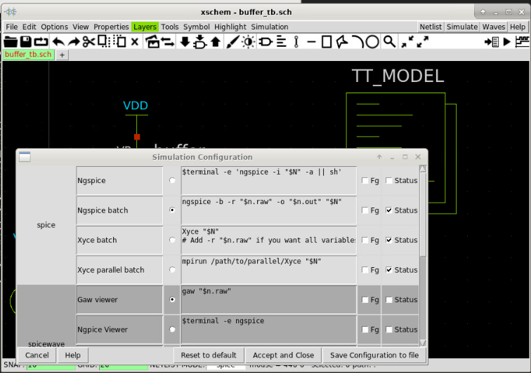
The simulation setup can be done by selecting Simulation >> Configure simulators and tools.
- In the
Ngspicesection, selectNgspice batchto use ngspice batch mode. - In the
Spicewavesection, selectGaw Viewer - Click on
Accept and Close. You can also save the simulation option by clicking onSave Configuration to file.
27. Simulate the design
To simulate the design, click on the Simulate button. If the Simulate button is red, the simulator is running.
When the simulation finishes, a new window will appear with the simulation status. You should review it to see if there is any problem during the simulation.
Simulation output
Completed: ngspice -b -r /home/cass/.xschem/simulations/buffer_tb.raw /home/cass/.xschem/simulations/buffer_tb.spice
data:

Note: No compatibility mode selected!


Circuit: ** sch_path: /home/cass/unic-cass/inverter/buffer_tb.sch

binary raw file "/home/cass/.xschem/simulations/buffer_tb.raw"
Doing analysis at TEMP = 27.000000 and TNOM = 27.000000

No. of Data Columns : 19

Initial Transient Solution
--------------------------

Node                                   Voltage
----                                   -------
x1.net1                                    1.8
vin                                          0
vdd                                        1.8
vout                               3.20523e-07
vin#branch                                   0
vdd#branch                        -4.71778e-10


No. of Data Rows : 2084

Total analysis time (seconds) = 0.053

Total elapsed time (seconds) = 5.651

Total DRAM available = 15402.340 MB.
DRAM currently available = 13993.477 MB.
Maximum ngspice program size =  153.195 MB.
Current ngspice program size =  138.066 MB.

Shared ngspice pages =    9.477 MB.
Text (code) pages =    5.496 MB.
Stack = 0 bytes.
Library pages =  137.043 MB.
Use Gaw to view the simulation waves
28. View the transient response
You can view the simulation results by clicking on the Waves button. A Gaw will be displayed with the recorded signals.
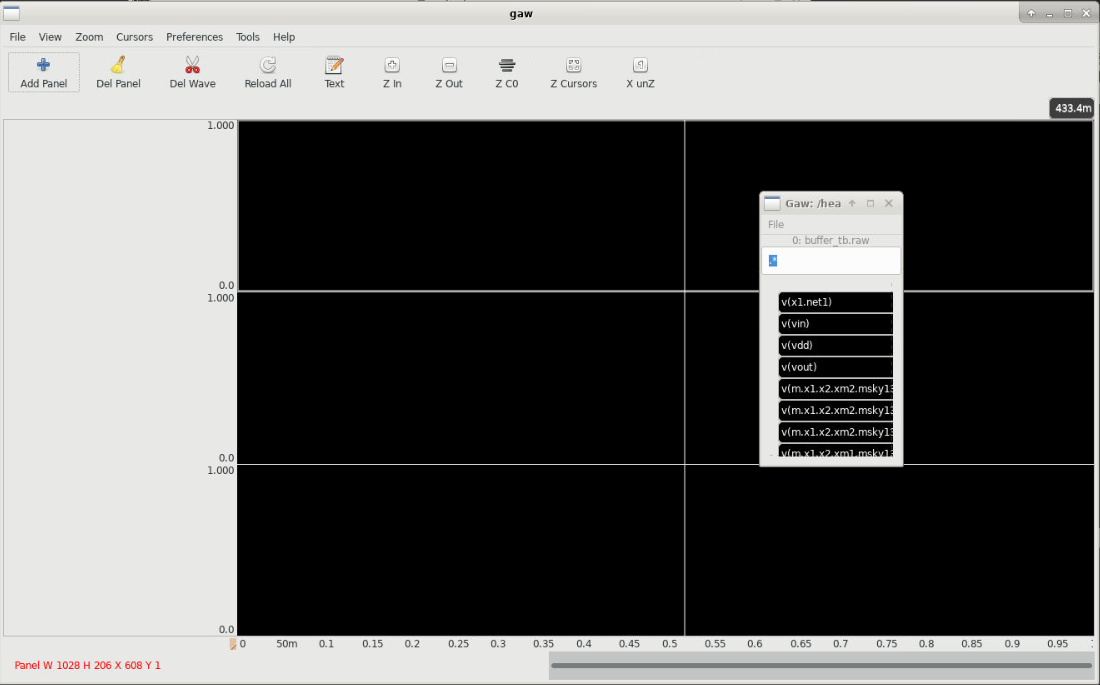
To add a signal to the wave viewer, you can click on a panel first, then add the signal in the signal list. For example, we add the Vin and Vout signals to the waveform as follows:
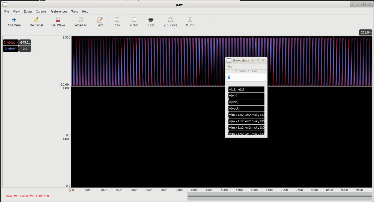
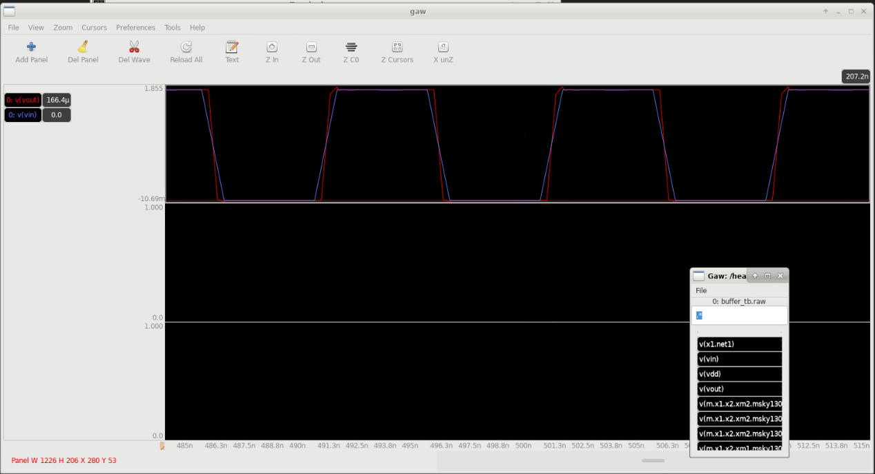
29. Zoom in and out
You can zoom in to see the delay between the input and the output after going through a buffer.
What’s next?
You’ve just finished the basic tutorials on how to create a hierarchical design. In the next lesson, we will use magic to create the design layout.