3.5 Layout an Inverter in IHP SG13G2 with KLayout including DRC and LVS
This section introduces how to layout the inverter in IHP SG130 PDK with KLayout including DRC and LVS.
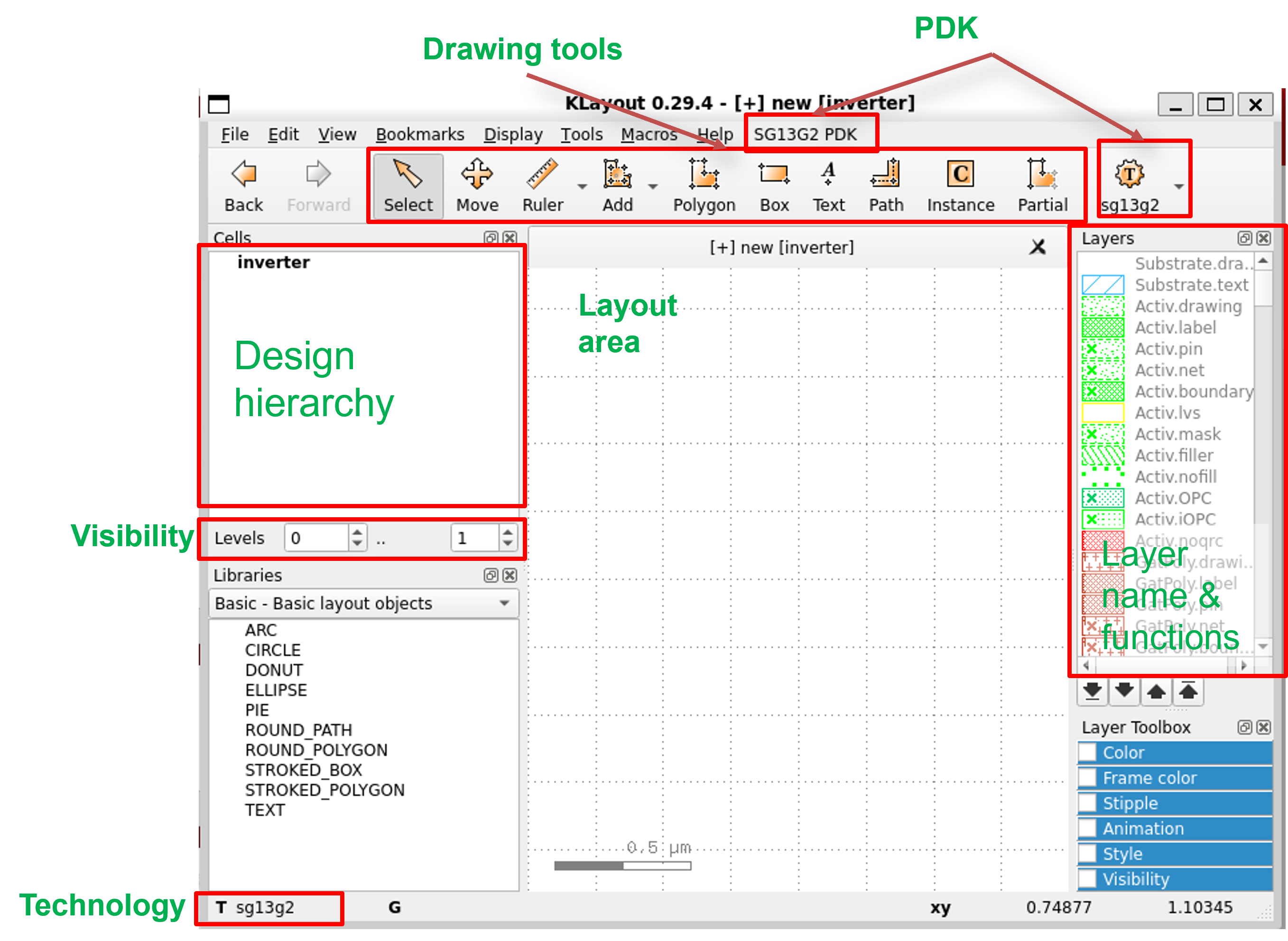
1. KLayout GUI
KLayout is capable of:
- Drawing layout of complex structures
Standard cells
Analog blocks
MEMs, etc.
- Parametric cell supports
Change cell parameters
-
Capability of doing DRC/LVS
-
Morden user interface
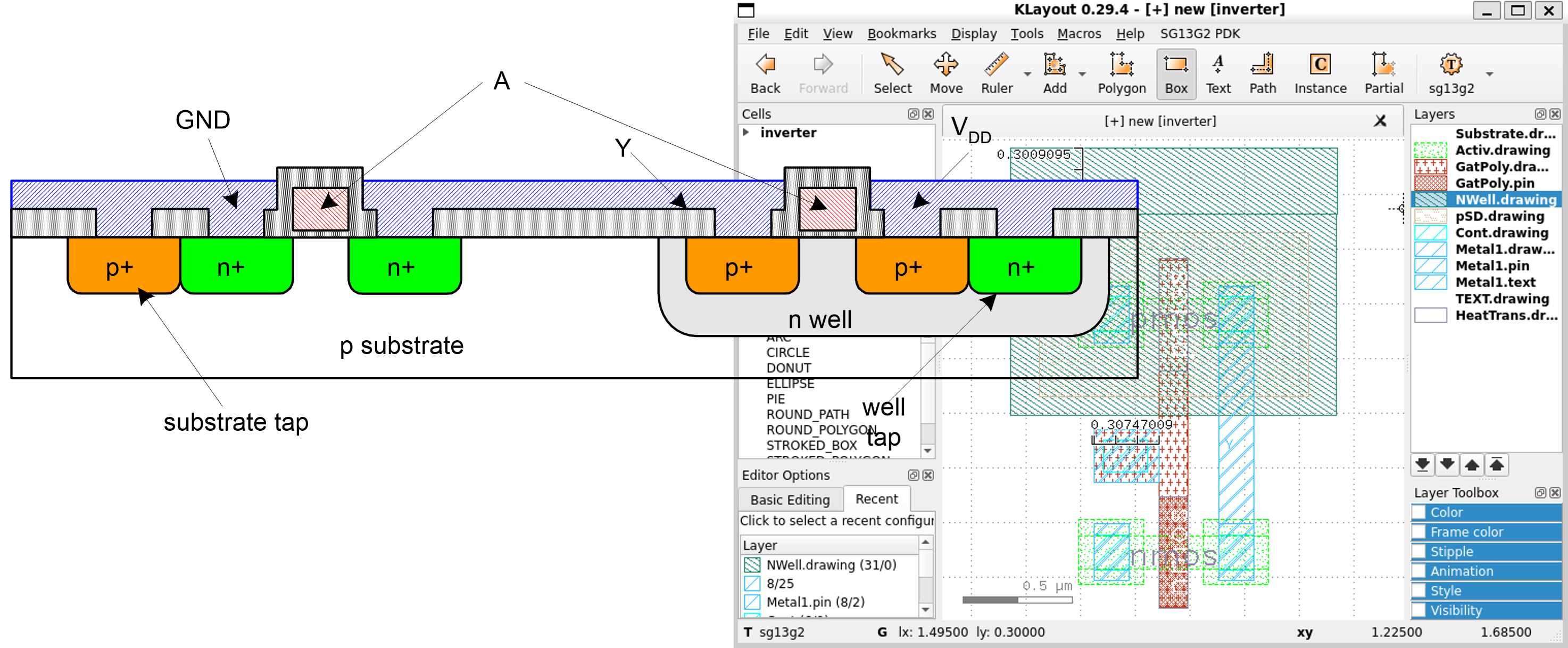
2. IHP-SG13G2 Process Cross Section
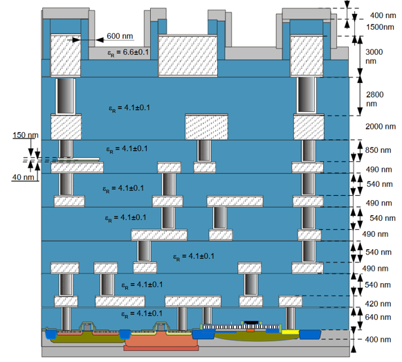
- BEOL detail cross-section below
Metal1for passive modeling
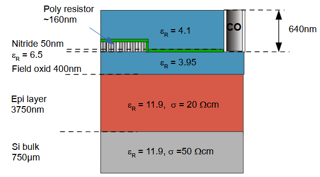
Remark:
-
ILDO consists of oxide (
590nm) and nitride (50nm) -
For a homogenous ILDO with
$$\varepsilon_R$$=4.1, the effective thickness corresponds todeff=620nm.
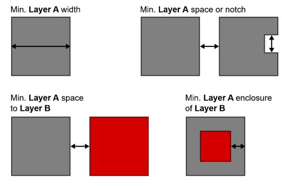
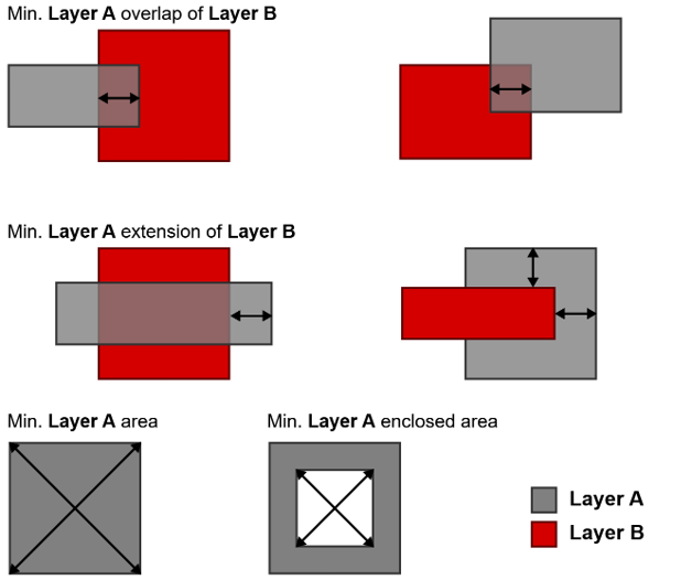
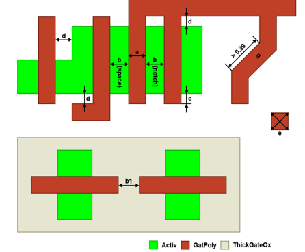
2.1. Design Rules in IHP-SG13G2 - Rule check schematics
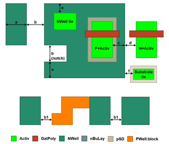
2.2. Design Rules in IHP-SG13G2 - NWell
| Rule | Description | Value (µm) |
|---|---|---|
| NW.a | Minimum NWell width | 0.62 |
| NW.b | Minimum NWell space or notch (same net). NWell regions separated by less than this value will be merged. | 0.62 |
| NW.b1 | Minimum PWell width between NWell regions (different net) (Note 3) | 1.80 |
| NW.c | Minimum NWell enclosure of P+Activ not inside ThickGateOx | 0.31 |
| NW.c1 | Minimum NWell enclosure of P+Activ inside ThickGateOx | 0.62 |
| NW.d | Minimum NWell space to external N+Activ not inside ThickGateOx | 0.31 |
| NW.d1 | Minimum NWell space to external N+Activ inside ThickGateOx | 0.62 |
| NW.e | Minimum NWell enclosure of NWell tie surrounded entirely by NWell in N+Activ not inside ThickGateOx | 0.24 |
| NW.e1 | Minimum NWell enclosure of NWell tie surrounded entirely by NWell in N+Activ inside ThickGateOx | 0.62 |
| NW.f | Minimum NWell space to substrate tie in P+Activ not inside ThickGateOx | 0.24 |
| NW.f1 | Minimum NWell space to substrate tie in P+Activ inside ThickGateOx | 0.62 |
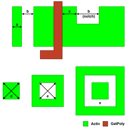
2.3. Design Rules in IHP-SG13G2 - Active
| Rule | Description | Value (µm) |
|---|---|---|
| Act.a | Minimum Activ width | 0.15 |
| Act.b | Minimum Activ space or notch | 0.21 |
| Act.c | Minimum Activ drain/source extension | 0.23 |
| Act.d | Minimum Activ area | 0.122 |
| Act.e | Minimum Activ enclosed area | 0.15 |
2.4. Design Rules in IHP-SG13G2 - GatPoly
| Rule | Description | Value (µm) |
|---|---|---|
| Gat.a | Minimum GatPoly width | 0.13 |
| Gat.a1 | Minimum GatPoly width for channel length of 1.2 V NFET | 0.13 |
| Gat.a2 | Minimum GatPoly width for channel length of 1.2 V PFET | 0.13 |
| Gat.a3 | Minimum GatPoly width for channel length of 3.3 V NFET | 0.45 |
| Gat.a4 | Minimum GatPoly width for channel length of 3.3 V PFET | 0.40 |
| Gat.b | Minimum GatPoly space or notch | 0.18 |
| Gat.b1 | Minimum space between unrelated 3.3 V GatPoly over Activ regions | 0.25 |
| Gat.c | Minimum GatPoly extension over Activ (end cap) | 0.18 |
| Gat.d | Minimum GatPoly space to Activ | 0.07 |
| Gat.e | Minimum GatPoly area | 0.09 |
| Gat.f | 45-degree and 90-degree angles for GatPoly on Activ area are not allowed | — |
| Gat.g | Minimum GatPoly width for 45-degree bent shapes if the bend GatPoly length is > 0.39 µm | 0.16 |
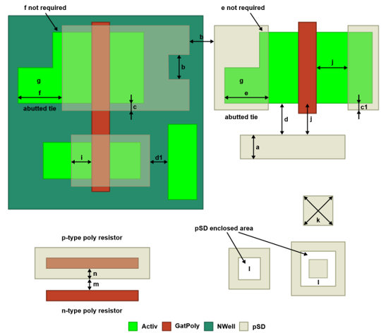
2.5. Design Rules in IHP-SG13G2 - pSD
| Rule | Description | Value (µm) |
|---|---|---|
| pSD.a | Minimum pSD width | 0.31 |
| pSD.b | Minimum pSD space or notch (Note 1) | 0.31 |
| pSD.c | Minimum pSD enclosure of P+Activ in NWell | 0.18 |
| pSD.c1 | Minimum pSD enclosure of P+Activ in PWell | 0.03 |
| pSD.d | Minimum pSD space to unrelated N+Activ in PWell | 0.18 |
| pSD.d1 | Minimum pSD space to N+Activ in NWell | 0.03 |
| pSD.e | Minimum pSD overlap of Activ at one position when forming abutted substrate tie (Note 2) | 0.30 |
| pSD.f | Minimum Activ extension over pSD at one position when forming abutted NWell tie (Note 2) | 0.30 |
| pSD.g | Minimum N+Activ or P+Activ area when forming abutted tie (Note 2) | 0.09 |
| pSD.i | Minimum pSD enclosure of PFET gate not inside ThickGateOx | 0.30 |
| pSD.i1 | Minimum pSD enclosure of PFET gate inside ThickGateOx | 0.40 |
| pSD.j | Minimum pSD space to NFET gate not inside ThickGateOx | 0.30 |
| pSD.j1 | Minimum pSD space to NFET gate inside ThickGateOx | 0.40 |
| pSD.k | Minimum pSD area | 0.25 |
| pSD.l | Minimum pSD enclosed area | 0.25 |
| pSD.m | Minimum pSD space to n-type poly resistors | 0.18 |
| pSD.n | Minimum pSD enclosure of p-type poly resistors | 0.18 |
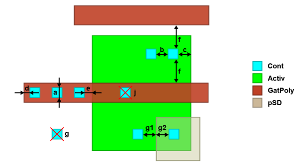
2.6. Design Rules in IHP-SG13G2 - Cont
| Rule | Description | Value (µm) |
|---|---|---|
| Cnt.a | Minimum and maximum Cont width | 0.16 |
| Cnt.b | Minimum Cont space | 0.18 |
| Cnt.b1 | Minimum Cont space in a contact array of more than 4 rows and more than 4 columns (Note 1) | 0.20 |
| Cnt.c | Minimum Activ enclosure of Cont | 0.07 |
| Cnt.d | Minimum GatPoly enclosure of Cont | 0.07 |
| Cnt.e | Minimum Cont on GatPoly space to Activ | 0.14 |
| Cnt.f | Minimum Cont on Activ space to GatPoly | 0.11 |
| Cnt.g | Cont must be within Activ or GatPoly | — |
| Cnt.g1 | Minimum pSD space to Cont on nSD-Activ | 0.09 |
| Cnt.g2 | Minimum pSD overlap of Cont on pSD-Activ | 0.09 |
| Cnt.h | Cont must be covered with Metal1 | — |
| Cnt.j | Cont on GatPoly over Activ is not allowed | — |
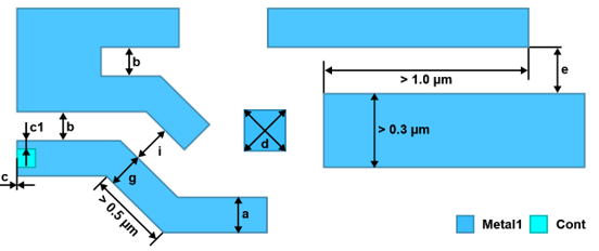
2.7. Design Rules in IHP-SG13G2 - Metal1
| Rule | Description | Value |
|---|---|---|
| M1.a | Minimum Metal1 width | 0.16 µm |
| M1.b | Minimum Metal1 space or notch | 0.18 µm |
| M1.c | Minimum Metal1 enclosure of Cont | 0.00 µm |
| M1.c1 | Minimum Metal1 endcap enclosure of Cont (Note 1) | 0.05 µm |
| M1.d | Minimum Metal1 area | 0.09 µm² |
| M1.e | Minimum space of Metal1 lines if at least one line is wider than 0.3 µm and the parallel run is more than 1.0 µm | 0.22 µm |
| M1.f | Minimum space of Metal1 lines if at least one line is wider than 10.0 µm and the parallel run is more than 10.0 µm | 0.60 µm |
| M1.g | Minimum 45-degree bent Metal1 width if the bent metal length is > 0.5 µm | 0.20 µm |
| M1.i | Minimum space of Metal1 lines of which at least one is bent by 45-degree | 0.22 µm |
| M1.j | Minimum global Metal1 density | 35.0 % |
| M1.k | Maximum global Metal1 density | 60.0 % |
3. Launch KLayout
- Run the following command in the terminal to launch
klayout.
$ source $HOME/unic-cass/env.sh
$ export KLAYOUT_PATH=$PDK_ROOT/$PDK/libs.tech/klayout:$HOME/.klayout
$ export KLAYOUT_HOME=$HOME/.klayout
$ klayout -e
4. Create a New Layout
Create a new layout by selecting File » New Layout and change the information as follows.
-
Technology:
sg13g2 - IHP SiGe 130nm technology -
Top cell:
inverter -
Database unit:
0.005
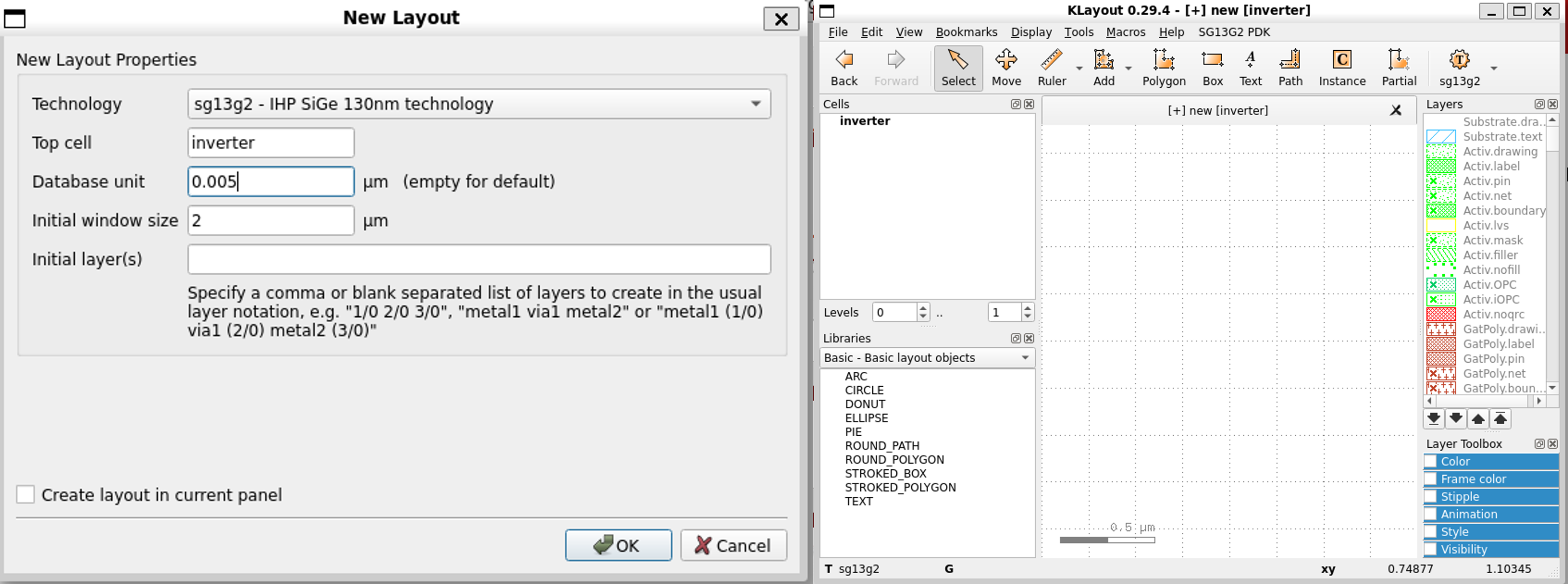
5. Create NMOS Instance
-
- Create a new
nmosinstance by clicking onInstacebutton
- Create a new
-
- In the instance dialog, select the
libraryasSG13_dev - IHP SG13G2 Pcells
- In the instance dialog, select the
-
- Click on
search button
- Click on
-
- Select
nmos, then pressOK
- Select
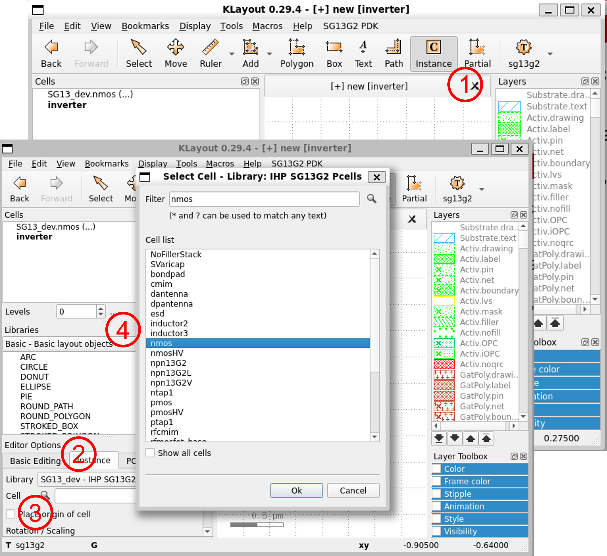
Finally, click on the layout to place the nmos.
6. Create PMOS Instance
-
- Create a new
pmosinstance by clicking onInstacebutton
- Create a new
-
- In the instance dialog, select the
libraryasSG13_dev - IHP SG13G2 Pcells
- In the instance dialog, select the
-
- Click on
search button
- Click on
-
- Select
pmos, then pressOK
- Select
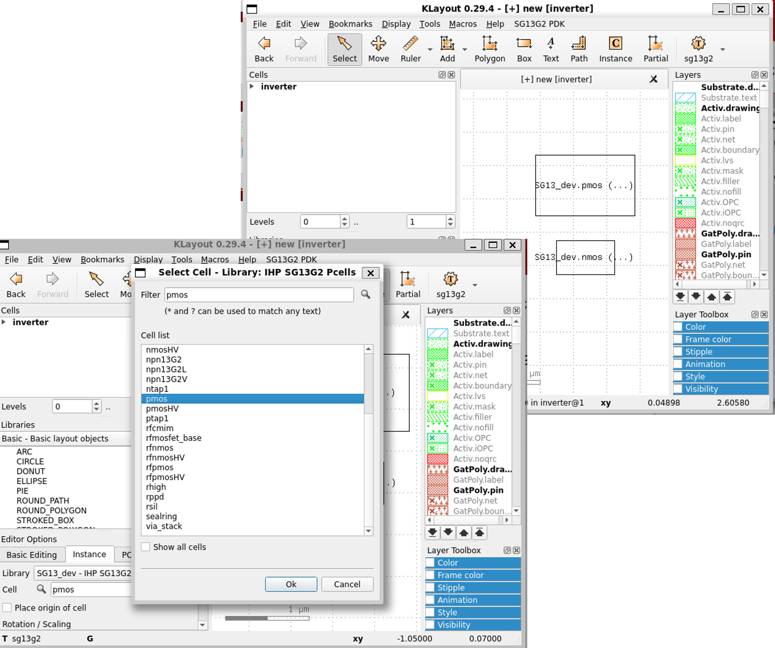
Finally, click on the layout to place the pmos.
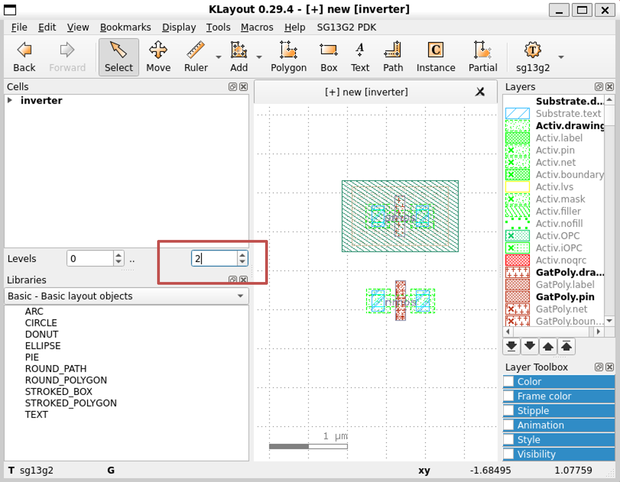
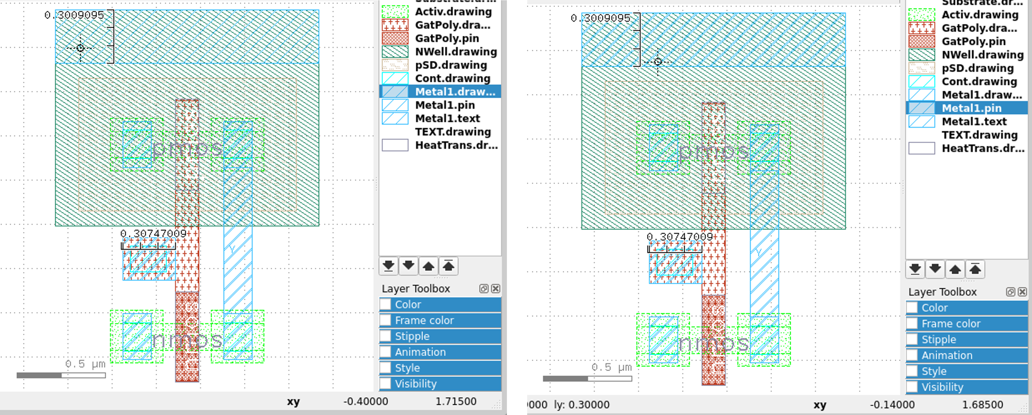
7. Change the Layout Visibility
- Display all the layer in the layout by changing the depth (e.g.:
2).
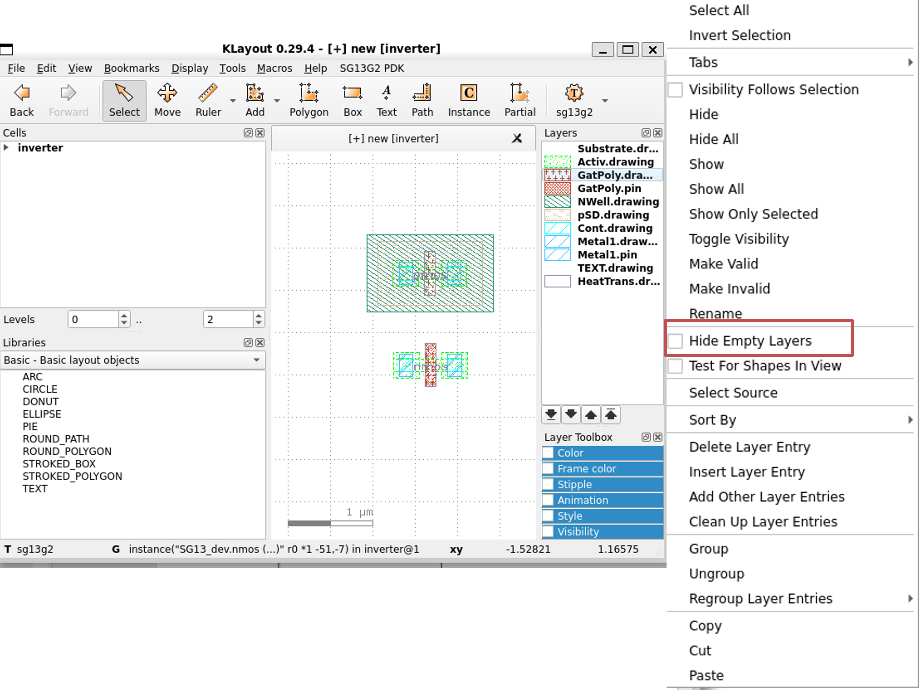
8. Hide Empty/Unused Layers
- Right click on
layerspanel and selectHide Empty Layers
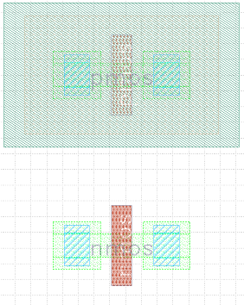
9. Align NMOS and PMOS
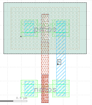
- Click on
Movebutton and move thepmossuch that thepolyof thepmosandnmosin the same line
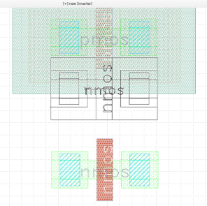
- Use the
arrowkeys on your keyboard to move thenmosdown.
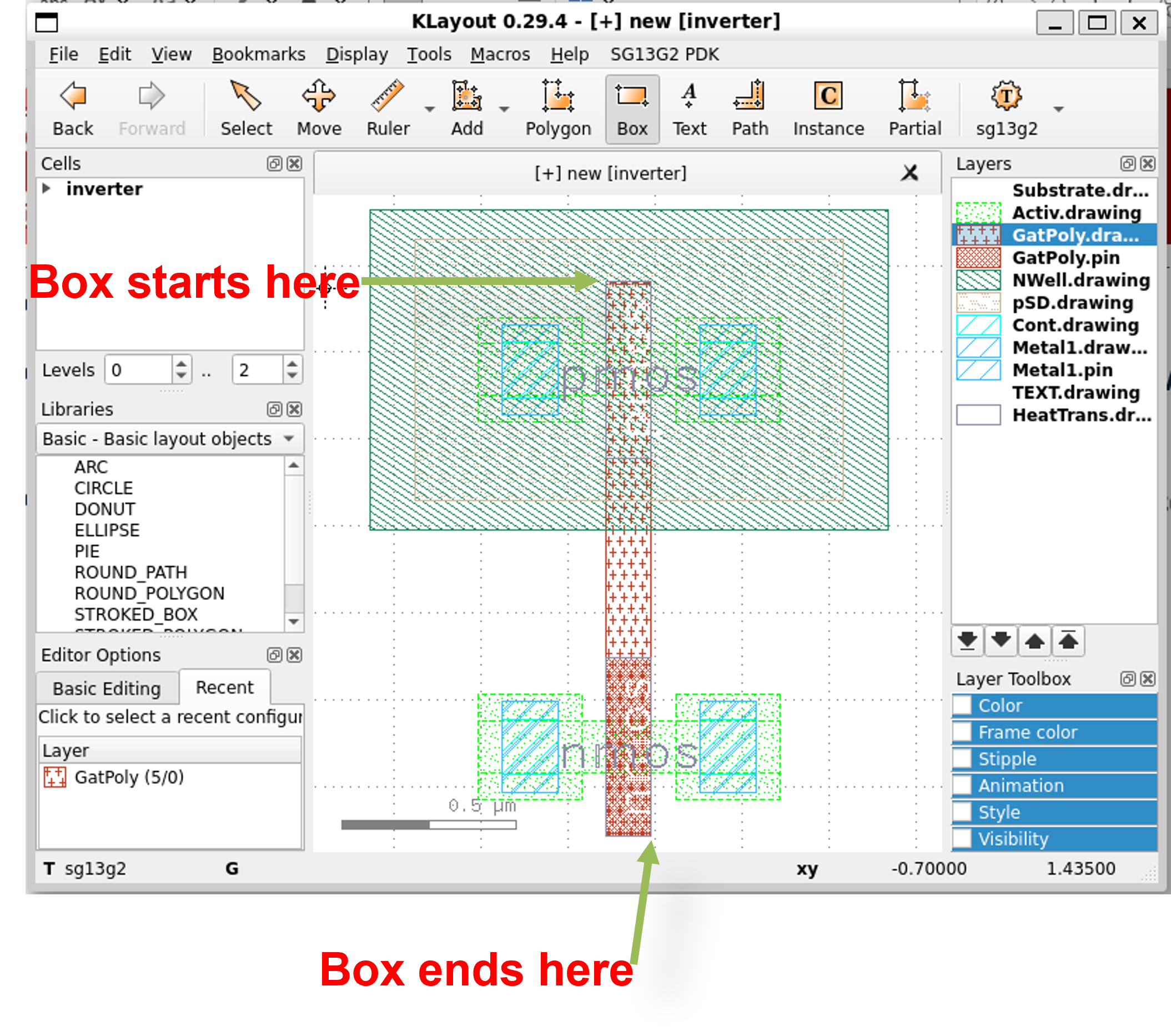
10. Connect the Poly
-
Click on
GatPoly.drawingin theLayerspanel -
Click on
Boxbutton then draw a box between the two poly
Note: The size needs to be exact as the one in the
pmosandnmos
- You can use zoom in and out to help place it correctly.
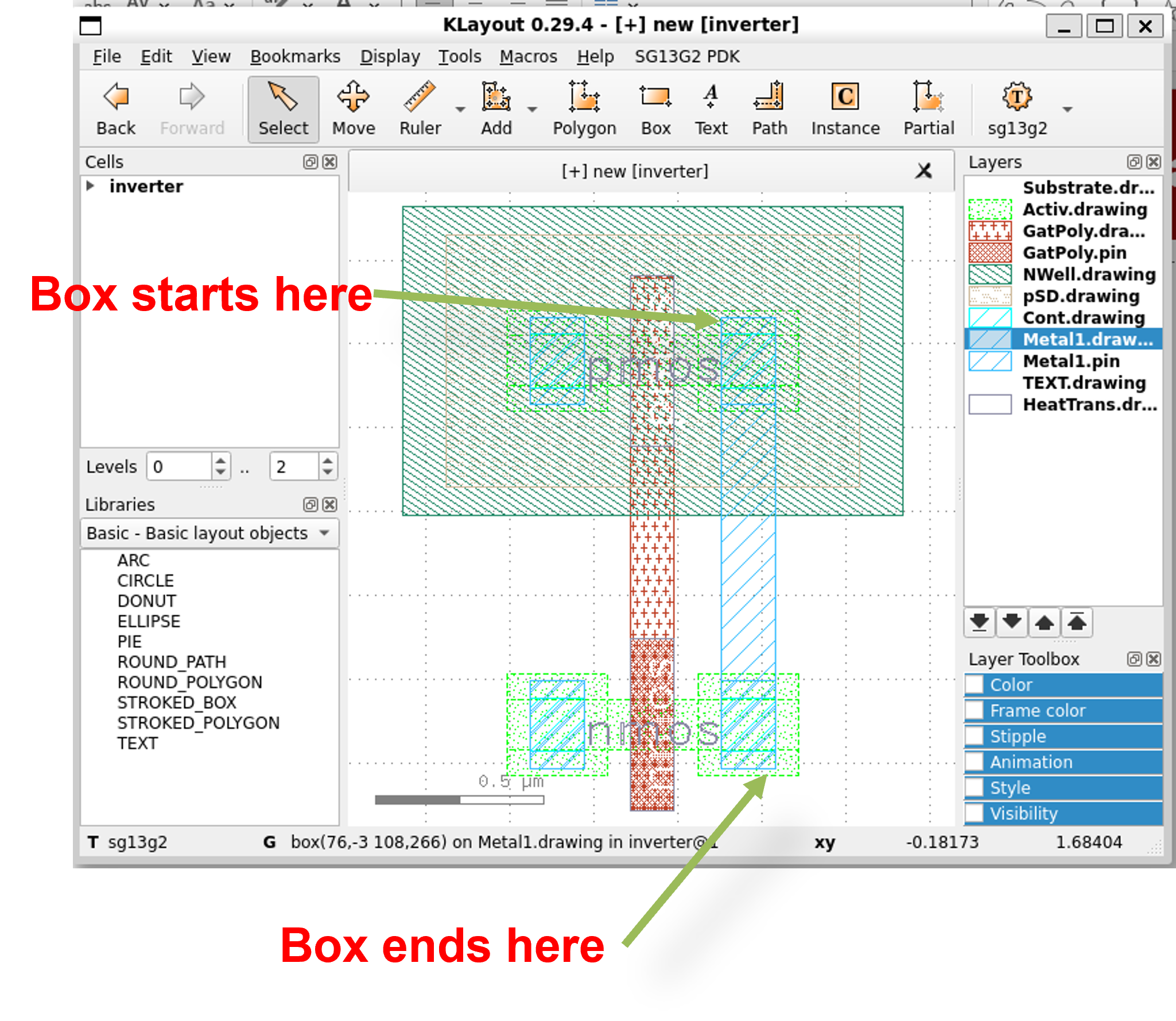
10. Connect the Terminals
-
Click on
Metal1.drawingon theLayerspanel -
Draw a box between two terminals by clicking on
Boxbutton and start drawing -
It should cover the two small box inside the
pmosandnmos
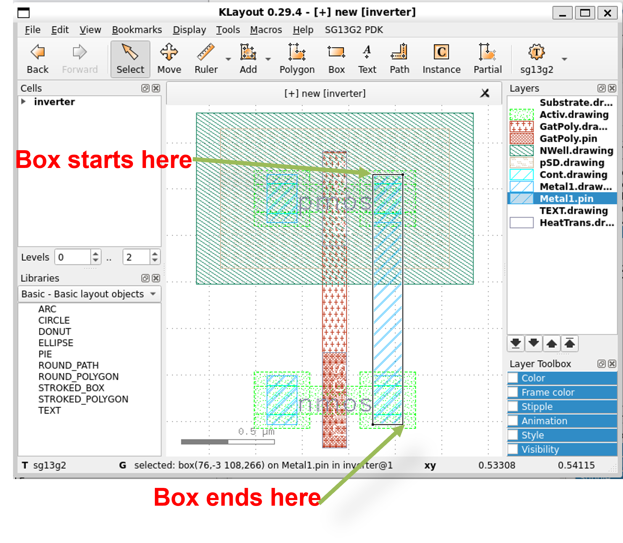
11. Create the Pins
- Click on
Metal1.pinon theLayerspanel and draw a box with the same size as the previous one
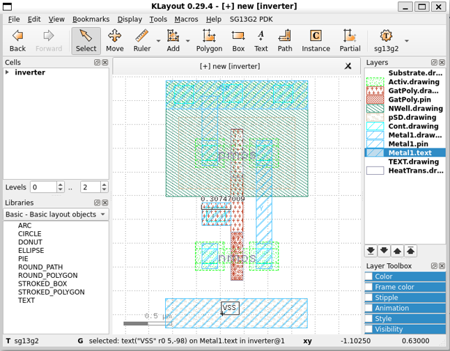
12. Change Pin Name
- Click on
Metal1.texton theLayerspanel
Right click on
Layerspanel » Uncheck hide empty layers
-
Click on the
textbutton and place it intoMetal1.pinregion (go back to select mode by pressesc) -
Double click on the text and change it into
Y
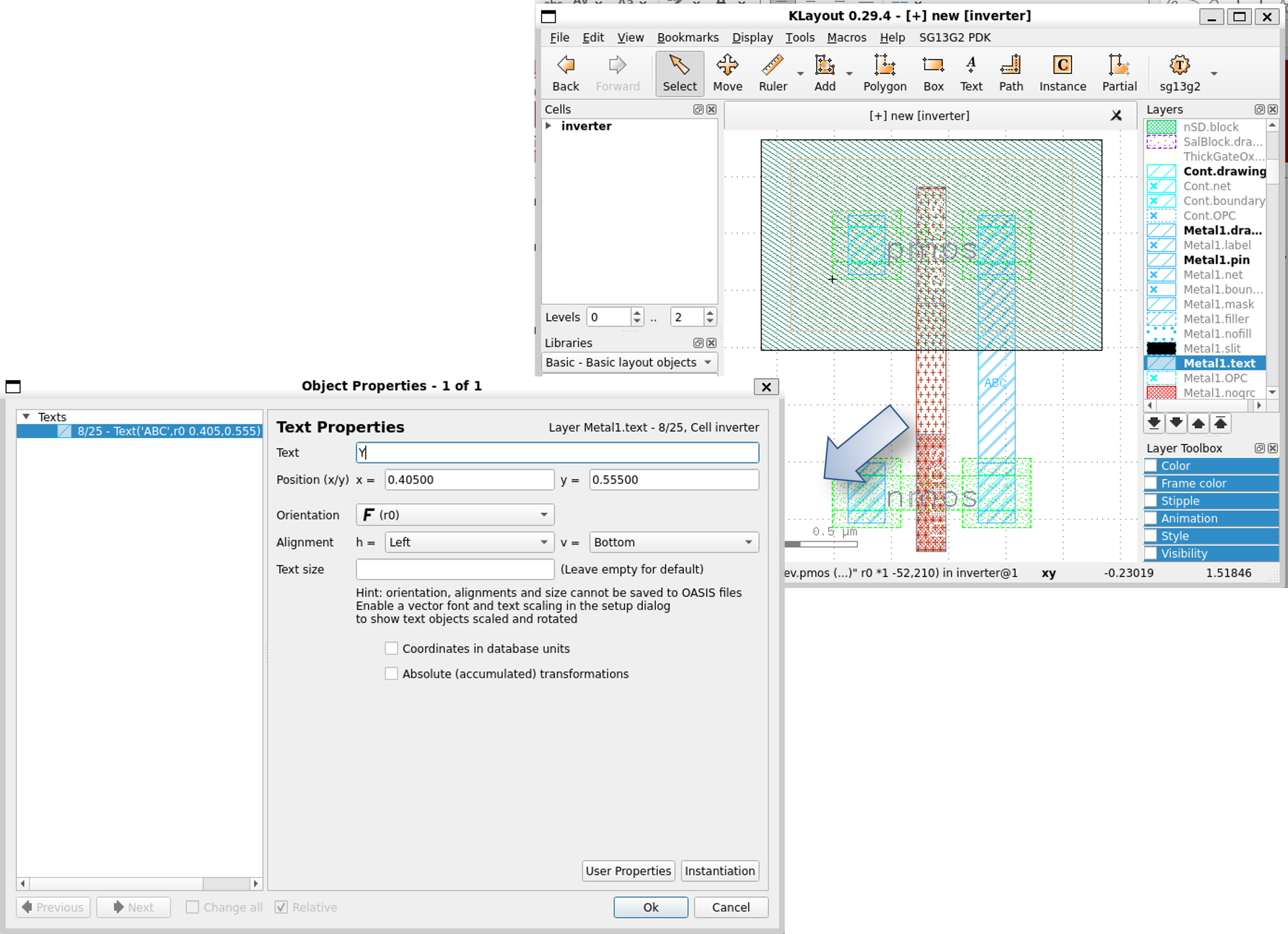
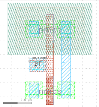
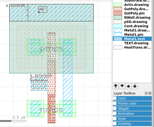
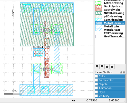
Final view is shown as follows.
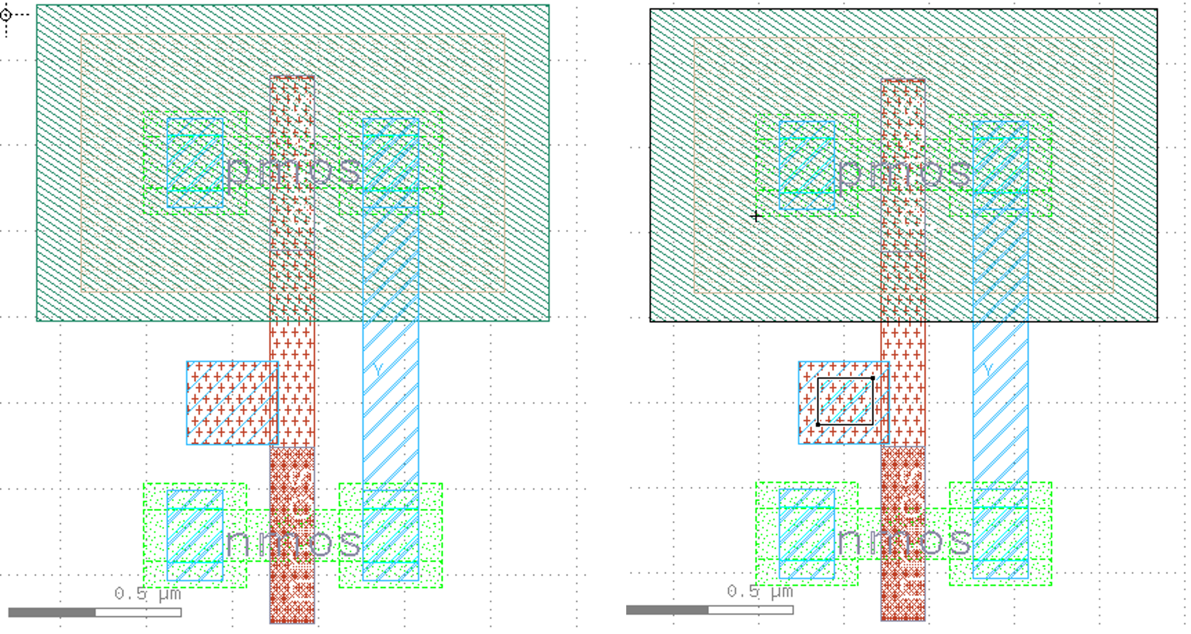
13. Connect Poly to Metal1
-
Click on
GatPoly.Drawingand draw a box of about0.2um x 0.2umto the gate terminal -
Draw a
Metal1over the above box with the same size
Click on
Metal1.drawingand draw a box
- Connect
MetaltoGatPoly
Click on
Cont.drawingand draw a small box inside
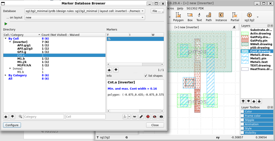
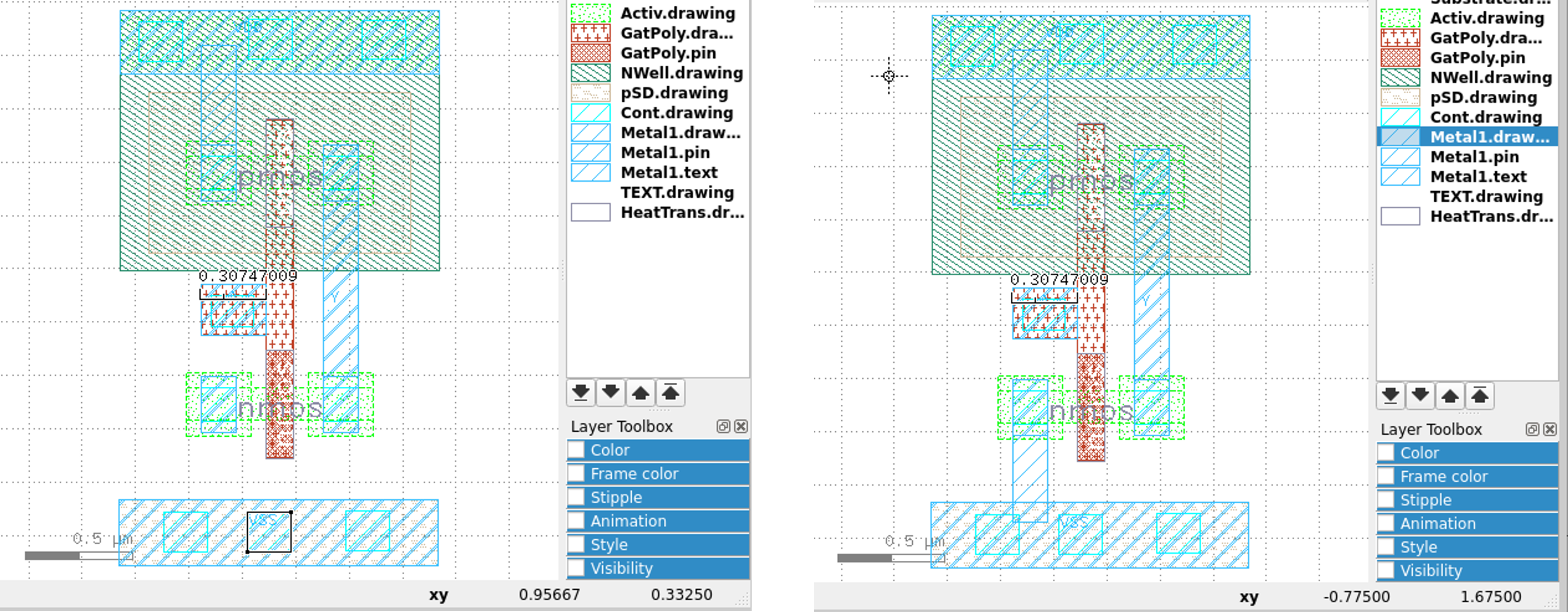
14. First DRC Check
-
Select
Tools»DRC»sg13g2_minimal.lydrc -
Click on the DRC violation, it will be highlighted in the layout view
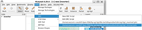
- In the figure,
M1.brule is violated, the minimumMetal1space or notch must be>=0.18um
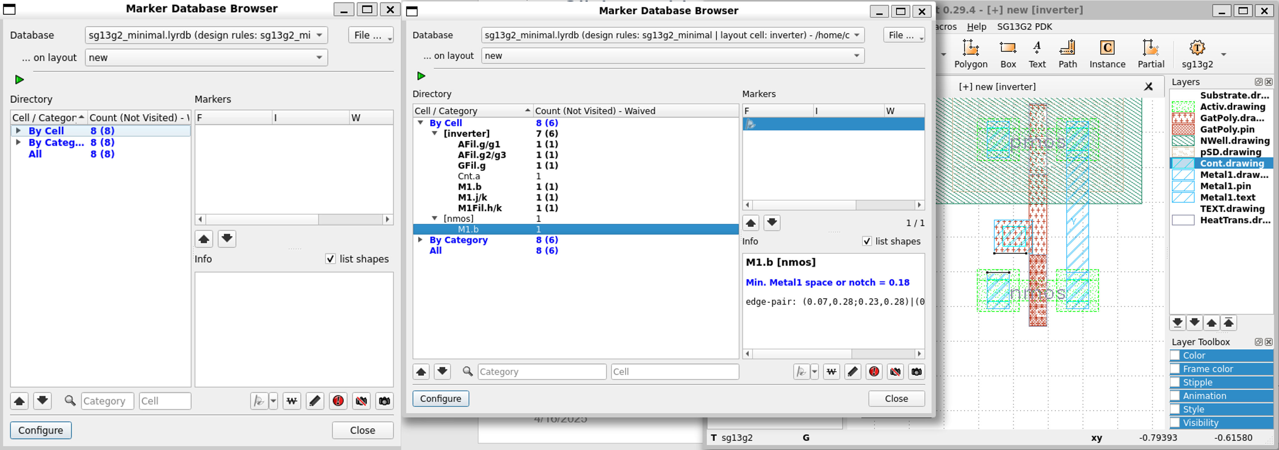
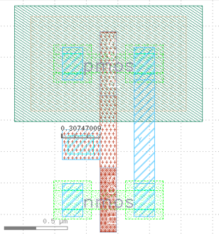
15. Second DRC Violation
- Rule
Cnt.ais violated the minimum and maximum contact width=0.16um
16. Fixed the DRC
- Delete the gate
polyand theMetal1and thecontact
Select the
gate poly,Metal1and theContactand pressDeletekey
- Draw a new one with bigger size
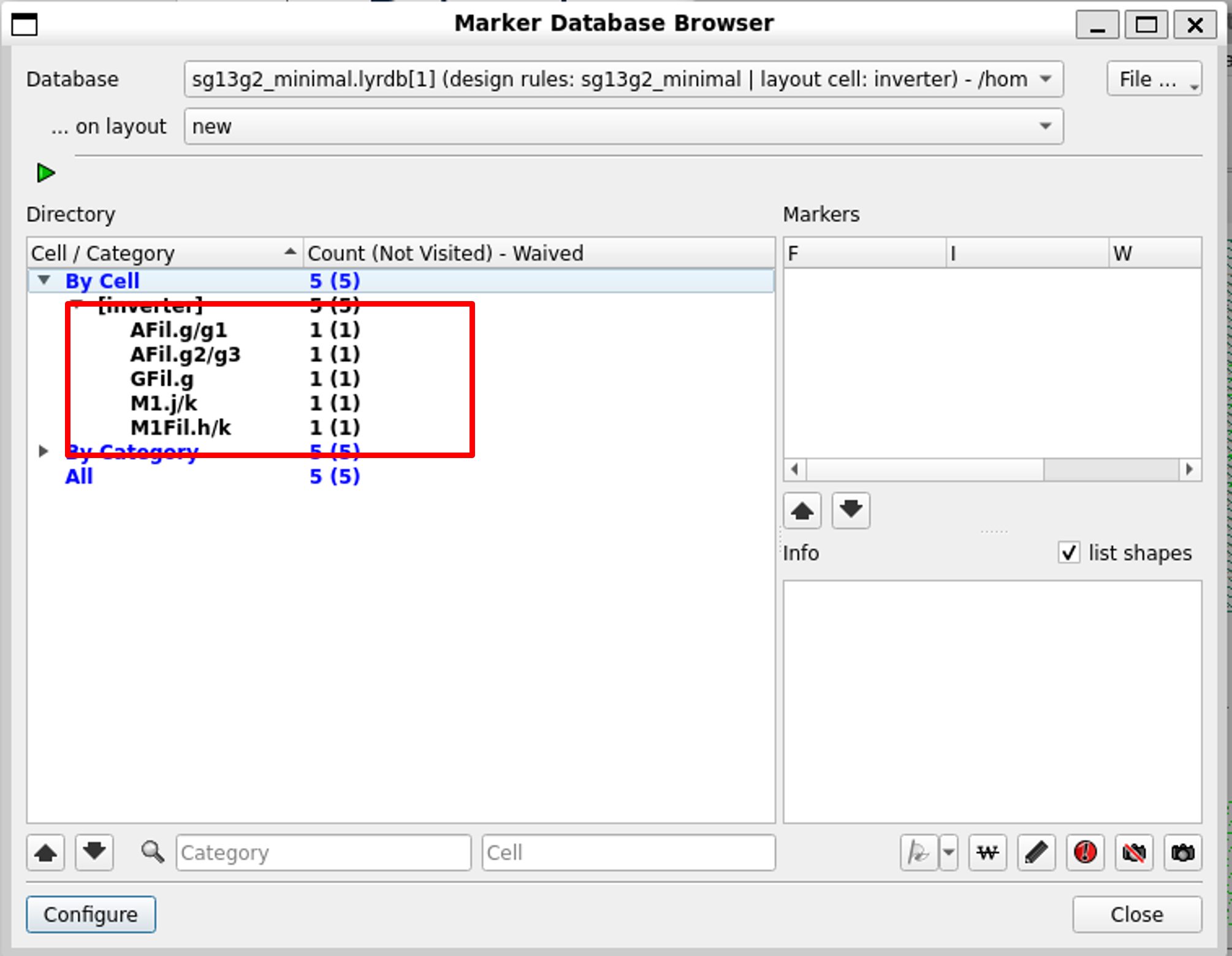
Note: You can use the ruler to have some idea of the size
- After completed, rerun the DRC, it passes
17. Create the A Pin
-
Select
Metal1.pinin theLayerspanel and draw a box with the same size as the previous one -
Select
Metal1.textin theLayerspanel and clickTextbutton to place the text inside the pin
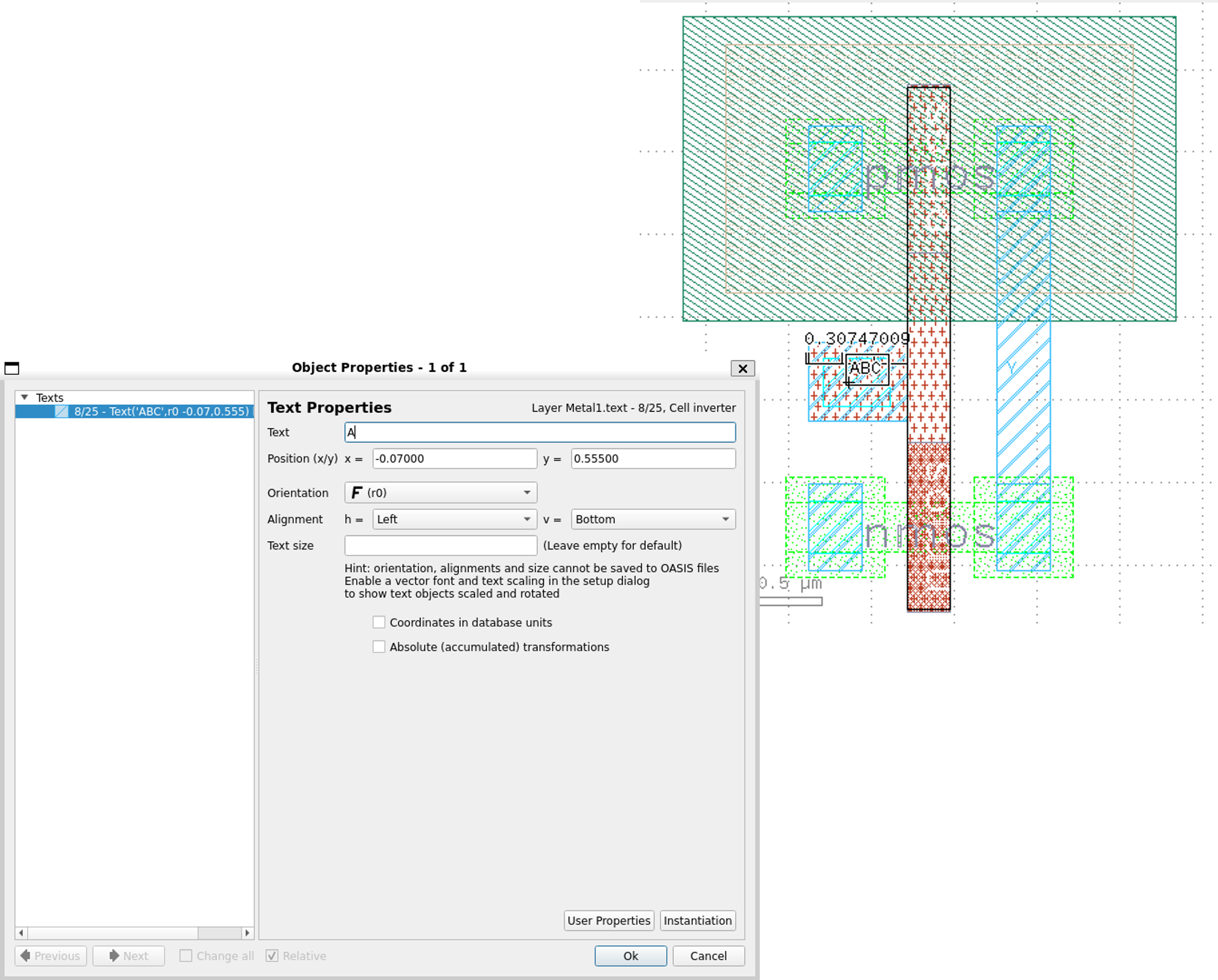
- Double click on the
textto change it intoA
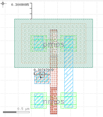
18. Extend the NWell for the PMOS
- Click on
Rulerand create a ruler approximately0.3umfrom the upper edge ofpmos
- Select
Nwell.drawingand draw a box to extend the nwell0.3umlong on thepmos
19. Create Metal 1
-
Select
Metal1.drawingand draw a box with the same size -
Select
Metal1.pinand draw a box with the same size
20. Create the VDD Text
-
Click on
Metal1.textand selectTextbutton -
Place the text inside
VDDpin -
Change the text to
VDD
21. Connect the Substrate and Terminal
-
Select
Act.drawingand draw a box with the same size asVDDpin -
Select
Cont.drawingand plot some small boxes inside theVDDpin region
Note that it must follow the DRC rule
- Select
Metal1.drawingand connect the terminal toVDDpin
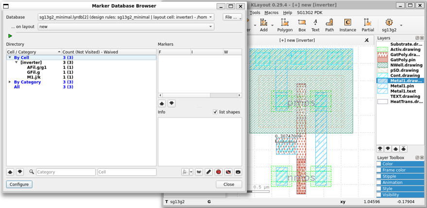
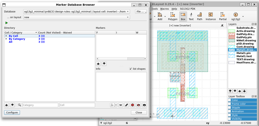
22. Run DRC Again
-
Run DRC by selecting
Tools»DRC»sg13g2_minimal.lydrc -
The results show that it is clean
We ignore three violation in the figure at this moment
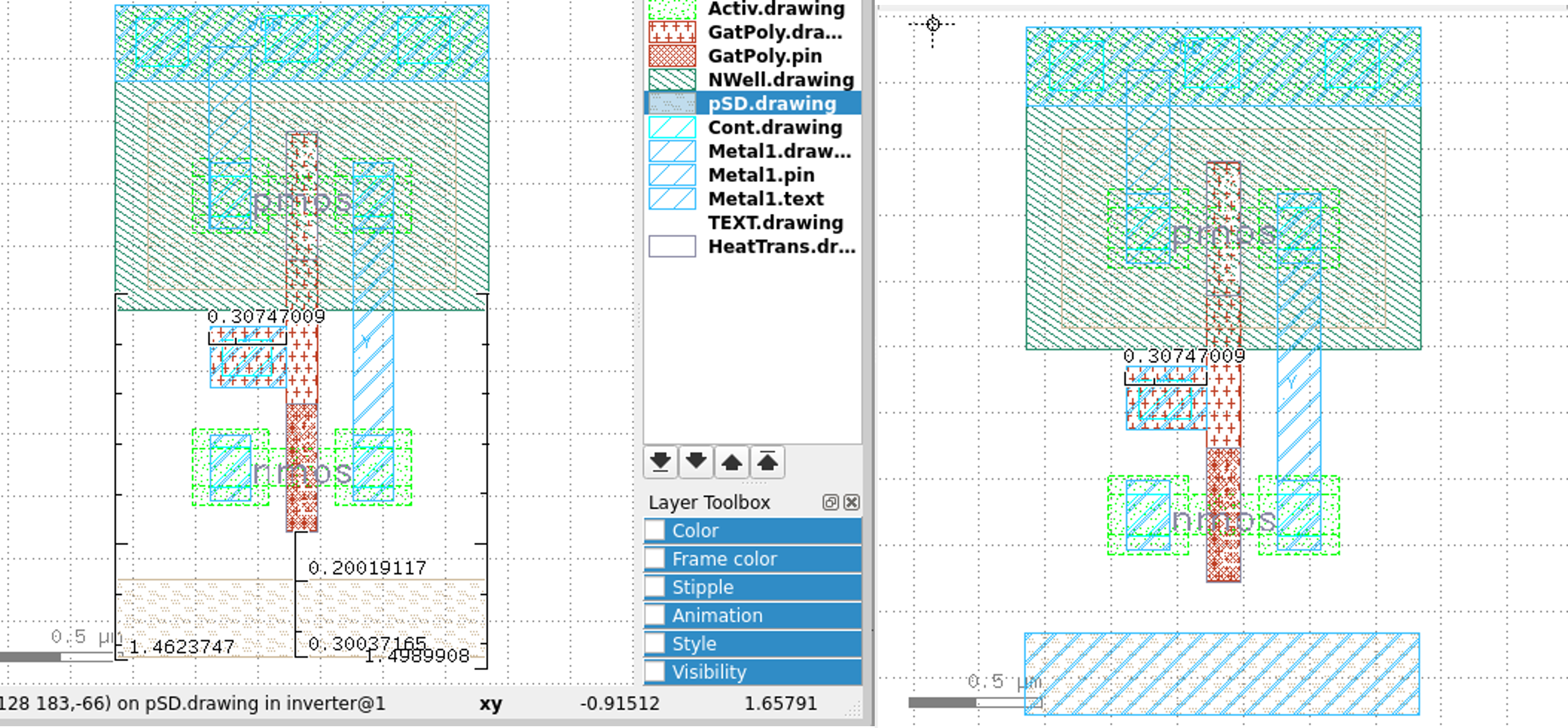
23. Draw pSD and Metal1
- Select
pSD.drawingand draw a box with the same size asVDDpin
You can use
rulerto help with the size
- Draw
Metal1.drawingandMetal1.pinwith the same size
24. Create VSS Text
- Select
Metal1.textand click ontextbutton, put the text insideVSSpin and name it asVSS
25. Connect VSS to the Substrate
-
Select
Cont.drawingand create some small boxes insideVSSpin -
Select
Metal1.drawingand create a shape connect to thenmos
26. Connect VSS to the NMOS
- Select
Metal1.drawingand create a shape connect to thenmos
27. Run DRC Again
- If there is no further DRC violation, the layout is done.
If there are a few, you will have to fix it.
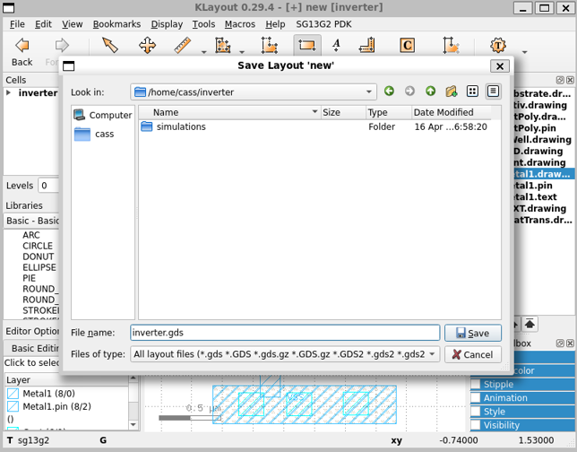
28. Save the Layout
- Click on
File»Save As. Store the files asinverter.gds
29. Export Netlist for LVS
-
Run
Xschemeand open theinverter.sch(that you have done inLab-04) -
Select
Simulation»LVS»LVS netlist: Top level is a .subckt -
Click on
Netlistbutton, it will generate a netlist in simulation folder
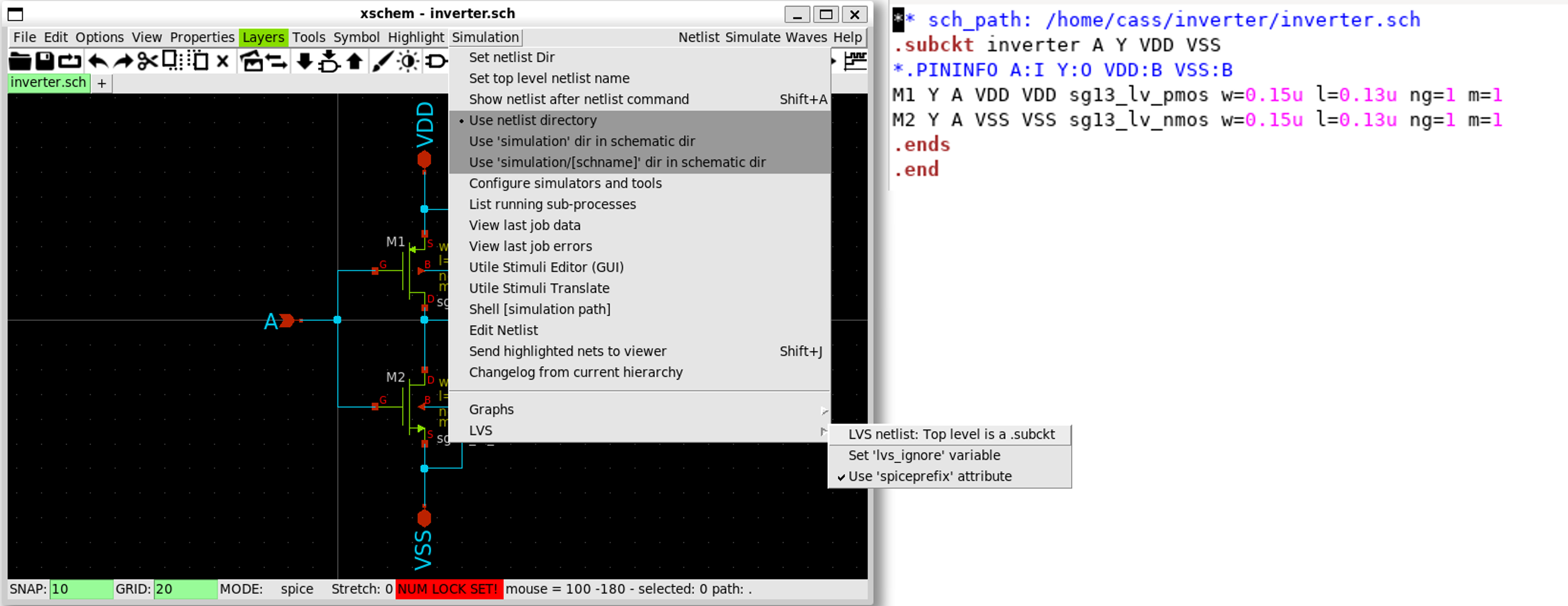
inverter
├── inverter.gds
├── inverter.sch
├── simulations
│   └── inverter.spice
└── xschemrc
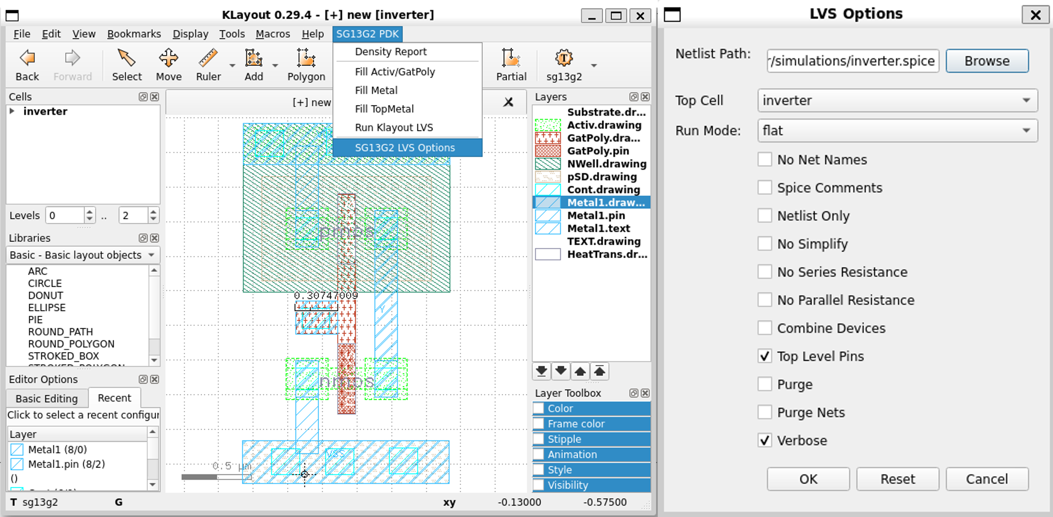
30. Setup the LVS
- Select
SG13G2 PDK»SG13G2 LVS Options
Set the netlist path as the netlist extracted from
ngspice
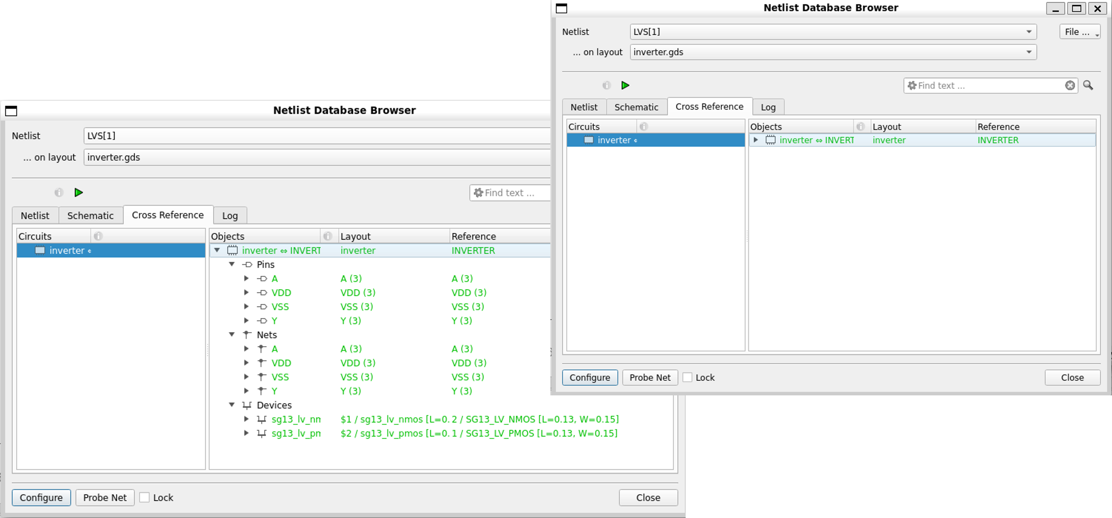
31. Run LVS
-
Select
SG13G2 PDK»Run LVS -
LVS should show that the circuit does not match (Layout does not match schematic)
We need to debug it. Scheme through the violations.
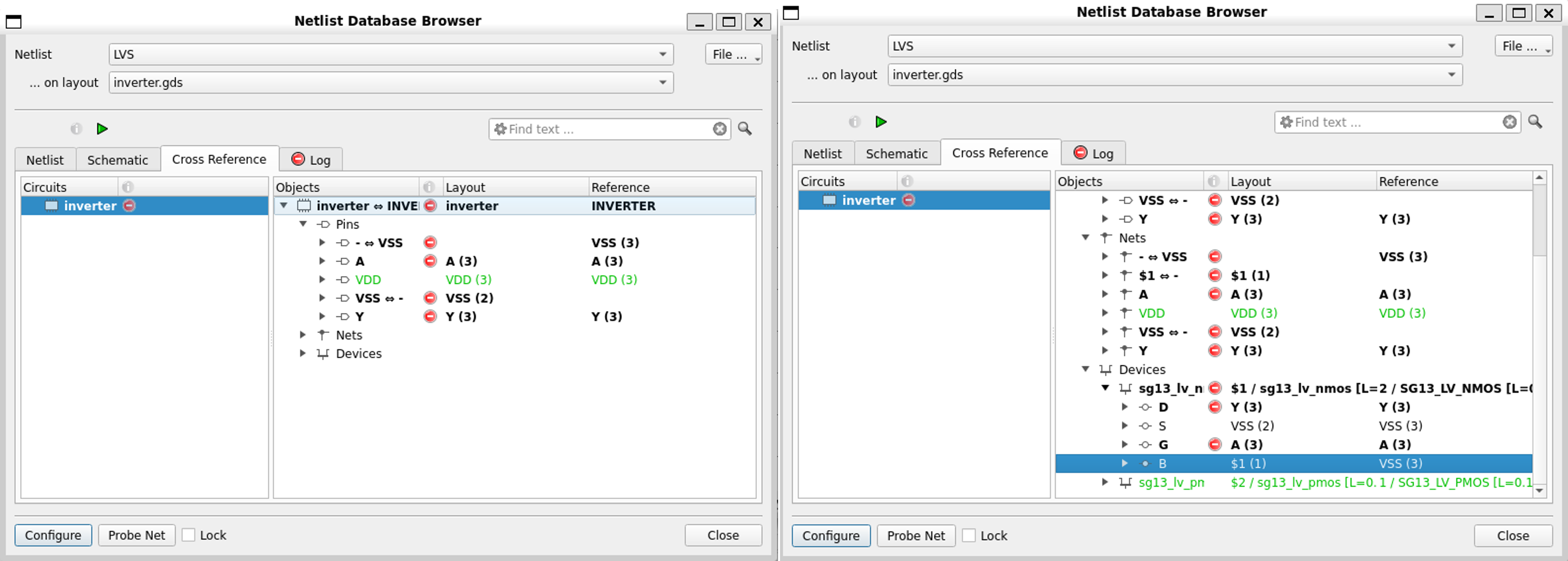
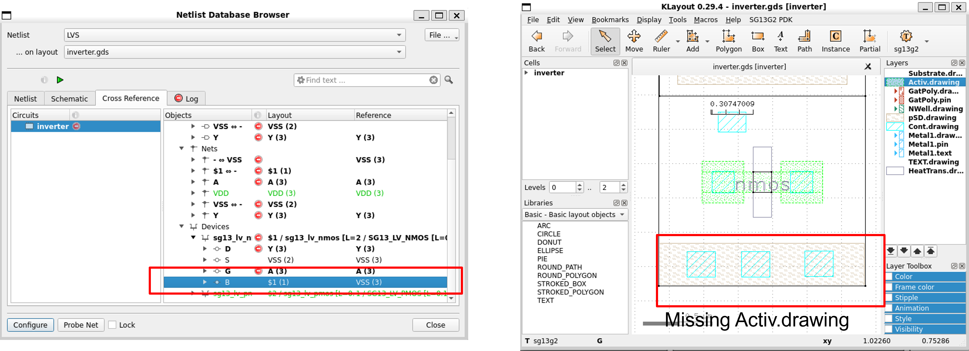
32. Find LVS Problems
- The problem is that the base terminal of the
nmosis not connected toVSS
This is because the
contactneedpSDandActivelayers.Activelayer is missing (verified on thelayout)
33. Fix the Layout
- Select
Activ.drawingand draw a box overVSSpin
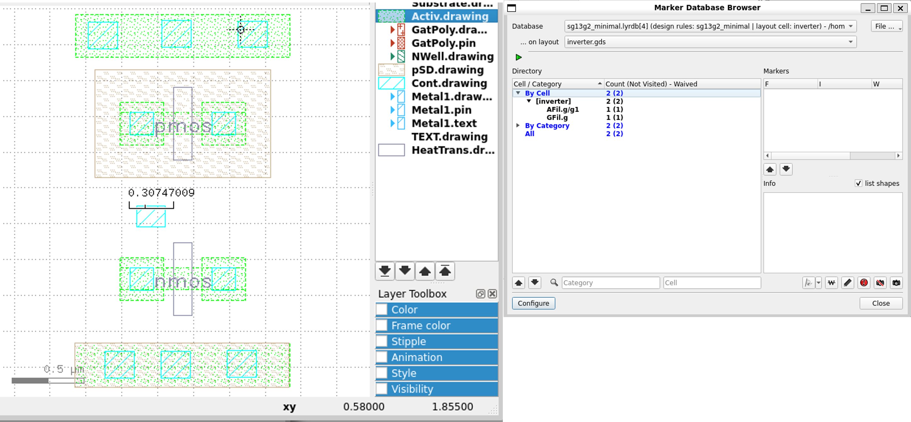
- Save
layoutand run DRC & LVS again
Finally, the LVS is clean as shown below.